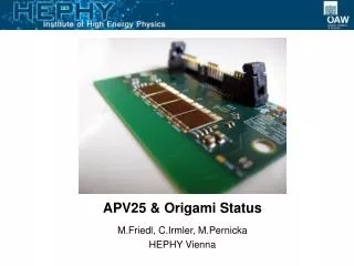
APV25 & Origami Status
160 likes | 346 Views
APV25 & Origami Status. M.Friedl, C.Irmler, M.Pernicka HEPHY Vienna. APV25 Purchase & Thinning. APV25 Purchase. Current Belle purchase 1500 diced „normal“ APV chips (~300µm thick) 2500 uncut APVs on wafers (for thinning) Future order

APV25 & Origami Status
E N D
Presentation Transcript
APV25 & Origami Status M.Friedl, C.Irmler, M.Pernicka HEPHY Vienna
APV25 Purchase & Thinning Markus Friedl (HEPHY Vienna)
APV25 Purchase • Current Belle purchase • 1500 diced „normal“ APV chips (~300µm thick) • 2500uncut APVs on wafers (for thinning) • Future order • 1000 more „normal“ APVs which did not fit in current purchase due to financial limits • 8 wafers with a total of 2674 known good dies were delivered to Vienna on 9 Jan 2009 • One wafer contains 360 APVs in total • Each chip was tested on the wafer, yielding an average of 93% good dies • The 1500 normal APVs are at KEK, financial transaction underway Markus Friedl (HEPHY Vienna)
APV25 Wafer Inspection APV25 wafers (8") Wafer map showing test results (used to ink mark bad dies on wafer) More photos: http://www.hephy.at/gallery2/v/electronics2/8inchwafer • On 19 Jan 2009, we sent 1 wafer (319 good dies) for • Thinning (100µm target), dicing and waffle packing • Received back on 4 Feb 2009 • 105µm (nominal) thickness • 314 (out of 319) good dies (= 98.4% yield) Markus Friedl (HEPHY Vienna)
Inspection of Thinned APVs Thickness measurement(Mitutoyo CMM) Waffle-packed thinned APV chips More photos: http://www.hephy.at/gallery2/v/electronics2/1stwaferthinned Markus Friedl (HEPHY Vienna)
Investigation of Thinned APV25 Chips • Thickness measurement: 106.6 +/- 3.2 µm • Thin dies are still quite rigid, easy handling thinning mechanically OK • Mounting 16 thinned chips on hybrids + 4 normal chips for electrical measurements • All perform equally well thinning electrically OK • Next step: populate 2 Origami modules, one with normal, one with thinned APVs • If again no difference, we will proceed with thinning all the chip-on-sensor wafers Markus Friedl (HEPHY Vienna)
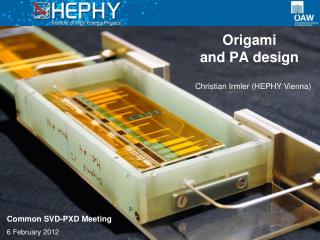
SVD Layout & Origami Markus Friedl (HEPHY Vienna)
Possible SuperSVD Layout • Geometry optimization is underway • Pixel double-layer using DEPFET • Strip layers extend to r~14 cm (presently 8.8 cm) • Every sensor is read out individually (no ganging) to maintain good S/N Origami concept for inner DSSDs (red) 4 layers of double-sided strip sensors Double-layer of DEPFET pixels More on the layout by Thomas Bergauer Markus Friedl (HEPHY Vienna)
Origami Chip-on-Sensor Concept Total material budget: 0.72% X0 (cf. 0.48% for conventional readout) • Kapton hybrid design for 4“ sensor done,being manufactured now • Design for assembly jigs is ongoing • Module to be constructed in April 2009 (readout connections not shown) Markus Friedl (HEPHY Vienna)
Origami – 4" DSSD Layout Connectors (on both sides) 2 p-side APV chips 2 p-side APV chips • 3-layer flex hybrid design • p- and n-sides are separated by 80V bias • n-side pitch adapter is integrated in hybrid • ordered at CERN PCB workshop, expected back ~end of March 4 n-side APV chips Animal farm (mascots:cat MF, eagle SS, bat CI) Flex fanouts to be wrapped around the sensor edge Markus Friedl (HEPHY Vienna)
APV25 Trigger, Clock and Dead Time Markus Friedl (HEPHY Vienna)
25.9 12.8 No External Restrictions • Min Lost: too little distance between triggers (6 clocks min.) • FIFO Lost: too many pending readouts (filling APV25 buffers) • Nakao-san wishes <3% dead time @ L1=30kHz • OK (0.87%) for 42.4MHz clock, slightly higher (3.43%) at 31.8MHz Markus Friedl (HEPHY Vienna)
External 500ns Dead Time Requirement (ECL) • Nakao-san‘s wish (<3% dead time @ L1=30kHz) met in both cases • 0.42% for 42.4MHz clock and 2.7% at 31.8MHz • 500ns dead time (as required by ECL) not accounted for APV25 • Hence minimum lost figure is always zero 24.0 11.4 Markus Friedl (HEPHY Vienna)
Summary & Outlook • APV Thinning • 1st wafer successfully thinned (16.6 µm) • Electric sample (~5%) tests are fine • Remaining APV wafers to be processed after successful tests on Origami • Origami Status • flex circuit design submitted for fabrication at CERN, expected back ~end March 2009 • Jig design underway, will assemble in April • Dead Time • Always <3% dead time with both42.4 and 31.8 MHz clocks in case of500 ns dead time requirement (ECL) Markus Friedl (HEPHY Vienna)
Backup Slides Markus Friedl (HEPHY Vienna)
Origami Concept • Extension of chip-on-sensor to double-sided readout • Flex fan-out pieces wrapped to opposite side (hence “Origami“) • All chips aligned on one side single cooling pipe Side View (below) Markus Friedl (HEPHY Vienna)