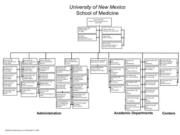
Download
1 / 23
230 likes | 251 Views
Explore cutting-edge sensor testing techniques conducted at University of New Mexico including visual, electrical, and mechanical quality assurance methods. Learn about production test stands, wafer testing, IV curves, capacitance scans, and more.

E N D
Sensor Testingat University of New Mexico C. Hägemann, M. Hoeferkamp, D. Fields, A. Zimmerman, M. Malik VTX Meeting 03 June 2005
Sensor QA Testing Sensor QA Testing – Visual Sensor QA Testing – Electrical Sensor QA Testing – Mechanical
Sensor QA Testing Sensor QA Testing – Visual Sensor QA Testing – Electrical Sensor QA Testing – Mechanical
Production Test Stand • Semiautomatic probestation, 2 Keithley 706 scanners with 10 and 3 Keithley7058 low current scanner cards respectively
Production Test Stand • Cleanroom
Visual Testing As seen before: Equipment is functional, Visual Testing can be easily performed Sintef Wafers: A1 and A3 are scratched; Not seen on the other wafers
Sensor QA Testing-Electrical • Test stand using scanner and probecard is fully operational • Tests that will be performed on the wafer: • Current Scan (Measure ILeak at each strip; VBias = const) • Capacitance Scan (Measure C at each strip; VBias = const) • IV Measurement (on 10% of the strips) • CV Measurement (on 10% of the strips)
Current Scan VBias = 100 V • 6 measurements total, each with 64 needles (melted needles on probe card) • Strip #3, 67, 131,…: either bad needle or bad cable
Current Scan • What is the difference between the 3rd measurement and the last three ?
Current Scan • Only 61 needles are actually touching pads • Change of the magnitude of the current by 100 → indicates bad strip?
IV • Characteristic IV curve of a p-n-junction • Def VBreak: Point where IV curve starts rising exponentially
IV VBreak ~ 320 V Def VBreak where I > 2.5*Inominal ~ 2.5nA
Capacitance Scan • OPEN correction accounts for test fixture on LCR meter • Measure Capacitance of each channel when needles are above the wafer No VBias • Plot Ccorr. = Cuncorr. – Ccorrection vs Channel Number
Capacitance Scan VBias = 150V • Same shape as data seen from BNL (~1pF; we don’t get any peaks in the middle) -> due to wafer / probecard?
Capacitance Scan • Same shape as data seen from BNL (~1pF; we don’t get any peaks in the middle) -> due to wafer / probecard?
CV • On each sensor, measure 10% of the strips • Substract Ccorrection for each particular strip measured • Inquire about AC frequency dependence of measured C first (LCR meter)
CV • Other wafers/channels look about the same
CV • Other wafers/channels look the same → Should use AC frequency of at least 10kHz
CV VDepletion ~ 70 V • Plot 1/C2 to find VDepletion • This defines VBias: 150 V or VDepletion + 50V
Sensor QA Testing-Mechanical • We have made wafer thickness and flatness measurements on the eight Pre Production wafers. • Use our E+H MX203 Contactless Wafer Geometry Gauge • Performs contactless measurements with capacitive sensors on both sides of wafer, there are no moving parts during measurement • Resolution 0.1 mm
Summary / Next Steps • Probestation is fully functional with all the VI’s working and tested • Compare VBreak and VDepletion for all the wafers • Investigate further into the effect of the guard ring on current scan • Once we get Hamamatsu wafers & new probe card - Compare measurements BNL – UNM - Remember: Need to normalize I to 20°C - Define what we mean with “bad sensor” - Start some thickness/flatness measurements