Download
1 / 36
360 likes | 396 Views
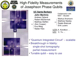
This collaboration between UC Santa Barbara and NIST in Boulder led by John Martinis and team presents high-fidelity measurements of Josephson phase qubits, showcasing breakthroughs in fidelity, tunable qubit technology, and single-shot tomography.

E N D
High-Fidelity Measurements of Josephson Phase Qubits UC Santa Barbara Collaboration with NIST – Boulder John Martinis Andrew Cleland Robert McDermott Matthias Steffen (Ken Cooper) Eva Weig Nadav Katz Markus Ansmann Matthew Neeley Radek Bialczak Erik Lucero GS PD UCR: A. Korotkov … UCI: C. Yu … • “Quantum Integrated Circuit” – scalable • Breakthrough in fidelity: • single-shot tomography • partial measurement • Tunable qubit – easy to use
= d d I I cos = d I I sin 0 j 0 º (1/L ) V F J = d 0 V = F0/2pI0cos d LJ p 2 nonlinear inductor 1 Gn+1 F 4 2 I 3 / 2 [ ] = - D 0 0 U 1 I / I ~ 1000 0 p 3 2 Gn E2 G2 0.9 1 / 2 æ ö p E1 1 / 4 2 2 I G1 [ ] ç ÷ w = - 0 1 I I ç ÷ w10 p 0 F C è ø E0 0 G0 w21 0.8 w32 0.7 0 5 ( ) - w E E / h + 1 n n p Qubit: Nonlinear LC resonator I R I0 LJ C U(d) <V> = 0 g10 wp DU <V> pulse (state measurement) 1: Tunable well (with I) 2: Transitions non-degenerate 3: Tunneling from top wells 4: Lifetime from R g10 @ 1 Lifetimeof state |1> RC
= s · · H I ( 2 ) x mwc · + s · 1.0 I y mws 0.8 ) ( dIdc(t) · + s · ¶ E / ¶ I / 2 dc 10 z 0.6 0.4 0.0 0.2 0.3 0.4 0.5 0.6 0.7 0.8 0.2 • State Preparation • Wait t > 1/g10for decay to |0> • Qubit logic with bias control • State Measurement: DU(I+Ipulse) • Single shot – high fidelity • Apply ~3ns Gaussian Ipulse Josephson-Junction Qubit potential |1> |0> I = Idc + dIdc(t) + Imwc(t)cosw10t+ Imws(t)sinw10t phase |0> |1> |2> 96% Prob. Tunnel • |1> : tunnel • |0> : no tunnel Ipulse I pulse (lower barrier)
IC Fabrication Qubit X,Y readout Imwave Is Z 100mm (old design) If junction via Al junction process & optical lithography Al Al SiNx Al Al2O3 substrate
X Y Imw Z Ip Reset Compute Meas.Readout time If Repeat 1000x prob. 0,1 Is 1 0 Vs Is Vs If Sequencer & Timer 300K V source ~10ppm noise ExperimentalApparatus rf filters fiber optics V source Ip ~10ppm noise Z, measure Imw X, Y I-Q switch mwaves 20dB 20dB 4K 20mK mw filters 20dB 10ns 3ns 30dB
Spectroscopy 6 2 P1 = grayscale Imw saturate few TLS resonances Ip meas. Microwave frequency (GHz) w10(I) Bias current I (au)
x y |0+|1 X |0+i|1 Y P1 State Tomography state tomography |0 |1 X,Y |0 DAC-I (Y) |1 DAC-Q (X) |0+ i|1 |0+ |1 • Good agreement with QM • Peak position gives state (q,f), • amplitude gives coherence
Standard State Tomography (I,X,Y) X Y I,X,Y |0+|1 P1 I time (ns)
Iw p Ip t 15 ns 10 ns State Evolution from Partial Measurement |0 Theory: A. Korotkov, UCR • “Look inside” • wavefunction projection • First POVM • in solid state |0+|1 Prob. = 1-p/2 “State tunneled” Prob. = p/2 state preparation partial measure p tomography & final measure
3/4 /2 /4 0 p=0.25 -10 p=0.75 -20 -30 Partial Measurement |0 qm p |0+|1
Decoherence and Materials Theory: Martin et al Yu & UCSB group Where’s the problem? Two Level States (TLS) Dielectric loss in x-overs TLS in tunnel barrier a-Al2O3 Im{e}/Re{e} = d = 1/Q future a- New design xtal Al2O3 <V2>1/2 [V]
LEED: Al Al2O3 Re Al2O3 (substrate) Spectroscopy: epi-Re/Al2O3 qubit mwave freq. (GHz) ~30x fewer TLS defects! Bias current I New Qubits I: Circuit II: Epitaxial Materials (NIST) SiNx capacitor 60 m (loss of SiNx limits T1)
Long T1 in Phase Qubits These results: Conventional design (May 2005): UCSB/NIST P1 (probability) T1 = 500 ns tRabi (ns) tRabi (ns) • T1 will be longer with better C dielectric • High visibility more useful than long T1
Coupled Qubits: i-SWAP gate PAB p tosc A B S 11 Probability PAB 01 10 p tosc 00 tosc i-SWAP gate: i-SWAP A CNOT gate with Tomography: B Turn interaction on/off with bias current
Coherence • T1 > 500 ns in progress, need to lengthen Tf • Breakthrough – decoherence from dielectric loss • STOP USING BAD MATERIALS! • Demonstrated improvements with new materials • Single Qubit operations work well • Tomography, partial measurement demonstrated • Coupled qubit experiment in DR • Simultaneous state measurement demonstrated • Violate Bell’s inequality soon • Tunable qubit : 4+ types of CNOT gates possible • Scale-up infrastructure (for phase qubits) Large C gives long-distance coupling • Optical Lithography – directly scalable • Large qubits - wiring straightforward • Wiring: 7 qubits/run tested, 100 possible in DR • Electronics working, scalable Future Prospects Very optimistic about 10+ qubit quantum computer
Reset Qubit operationMeasurementReadout time If Qubit Cycle If U(d)
Reset Qubit operationMeasurementReadout Qubit OpMeasAmp time If Qubit Cycle If U(d) … fast decay ~2000 states
Reset Qubit operationMeasurementReadout Qubit OpMeasAmp time If Qubit Cycle If U(d) “0” … fast decay ~2000 states “1” 1 F0
Reset Qubit operationMeasurementReadout Qubit OpMeasAmp time If Qubit Cycle If Measure p1 Is U(d) Is “0” … fast decay ~2000 states “1” 1 F0 Switching current 10 mA SQUID flux 0
Cc A B Coupled Qubits: Spectroscopy A C Cc 11 Off Resonant: 01 10 B 00 B qubit unbiased: A qubit unbiased: wA/2p (GHz) wB/2p (GHz) Flux Bias A Flux Bias B
Cc A B Coupled Qubits: Spectroscopy A C Cc 11 Resonant: 01 10 B 00 Moves with bias on B B qubit biased: A qubit unbiased: wA/2p (GHz) wB/2p (GHz) S= 74 MHz Flux Bias A Flux Bias B
Coupled Qubits: “i-swap” gate (in time domain) PAB p tosc A B 11 S 01 10 Probability PAB p tosc 00 Magnitude consistent with single qubit fidelity, mw drive xtalk tosc
Cross Coupling when Measurement is Delayed Qubit gate easy to make, During measurement coupling still on ! Measurement of 1 state dissipates energy Fixed Coupling: p p p A B P01same P10same P10 P01 P11 P11 When measure 1 state: pumps energy into 2nd qubit, producing 0 -> 1 transition
I(t)=CxdV/dt theory: V(t) Time Scale of Measurement Crosstalk experiment: V(t) 1 0 16 GHz I(t) on resonance Small crosstalk for misalignment <1 ns E/E10 t [ns]
Next Project: CNOT gate with tomography i-swap experiment CNOT (+ swap) gate p A A B B pulse iswap meas. X 0 0 Change pulse to vary initial state Change pulse to vary measurement basis
Dielectric Loss in CVD SiO2 Pin Pout HUGE Dissipation C L T = 25 mK Pin lowering Im{e}/Re{e} = d = 1/Q Pout [mW] <V2>1/2 [V] f [GHz]
Theory of Dielectric Loss E Amorphous SiO2 Two-level (TLS) bath: saturates at high power, decreasing loss high power Im{e}/Re{e} = d = 1/Q SiO2(100ppm OH) von Schickfus and Hunklinger, 1977 Bulk SiO2: SiO2(no OH) <V2>1/2 [V]
Theory of Dielectric Loss E Amorphous SiO2 • Spin (TLS) bath: saturates at • high power, decreasing loss high power Im{e}/Re{e} = d = 1/Q von Schickfus and Hunklinger, 1977 Bulk SiO2: <V2>1/2 [V] SiNx, 20x better dielectric Why?
Junction Resonances = Dielectric Loss at the Nanoscale New theory (suggested by I. Martin et al): 70 m2 70 m2 avg. 5 samples: Al 2-level states (TLS) . e d 1.5 nm wave frequency (GHz) AlOx N/GHz (0.01 GHz < S < S') 13 m2 Al S/h theory 13 m2 qubit bias (a.u.) splitting size S' (GHz) d=0.13 nm (bond size of OH defect!) Explains sharp cutoff Smax in good agreement with TLS dipole moment: Charge (not I0) fluctuators likely explanation of resonances
Junction Resonances: Coupling Number Nc Number resonances coupled to qubit: S 1 e E10 g 0 Statistically avoid with Nc << 1 (small area) qubit junction resonances … Nc >> 1, Fermi golden rule for decay of 1 state: Same formula for di as bulk dielectric loss Implies di = 1.6x10⁻³, AlOx similar to SiOx (~1% OH defects)
State Decay vs.Junction Area Monte-Carlo QM simulation: (p-pulse, delay, then measure) probability P1 A=260 um2 (Nc=1.7) A=2500 um2 (Nc=5.3) time (ns)
State Decay vs.Junction Area Monte-Carlo QM simulation: (p-pulse, delay, then measure) Nc2/2 A=18 mm2 (Nc=0.45) probability P1 A=260 mm2 (Nc=1.7) A=2500 mm2 (Nc=5.3) time (ns) Need Nc < 0.3 (A < 10 mm2) to statistically avoid resonances ~ ~
State Measurement and Junction Resonances Number resonances swept through: 1 tp Couple to more resonances 0 qubit junction resonances … Nc’ >> 1, Landau-Zener tunneling: (10 ns)-1 With tp ~ 10 ns, explains fidelity loss in measurement!
P = 0 P = 0.25 P = 0.96 Ptunneling 1.0 Experiment Theory 0.0
Infrastructure: Cryogenics Installed, working by 2/05 Redesign pot, precooler/shields New (dense) wiring design Microwave Nb, CuNi coax • Dilution Refrigerator for QC: • <20 mK base temp. • 10-100x wiring area • Shielding • (Fast cooldown, 16 hr) • (Low operation cost, 6 l/d) • Wiring for 100+ qubits
D/A Converter Microwave Bessel filter quadrature mixer N/A FPGA Sequencer Control PC Infrastructure: Electronics 100Mbit Ethernet 200MHz64bit bus,400KHzI2C bus SMAcables Software more difficult N/A Hardware modifications more difficult Example: Spin Lock 0 20 40 time (ns) p/2, 0° p, 90° p/2, 0°