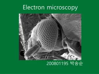
Plasmon Charge Density Probed By Ultrafast Electron Microscopy
260 likes | 706 Views
UST. PHYSICAL BIOLOGY Center for ULTRAFAST SCIENCE & TECHNOLOGY. Plasmon Charge Density Probed By Ultrafast Electron Microscopy. Sang Tae Park and Ahmed H. Zewail California Institute of Technology. 2013.12.09. Femtosecond Electron Imaging and Spectroscopy Workshop. Outline.

Plasmon Charge Density Probed By Ultrafast Electron Microscopy
E N D
Presentation Transcript
UST PHYSICAL BIOLOGY Center for ULTRAFAST SCIENCE & TECHNOLOGY Plasmon Charge Density Probed By Ultrafast Electron Microscopy Sang Tae Park and Ahmed H. Zewail California Institute of Technology 2013.12.09. Femtosecond Electron Imaging and Spectroscopy Workshop
Outline • Structural dynamics • ultrafast electron microscopy • design • capability • Visualization of plasmons • photon-induced near field electron microscopy • interaction of electron and (plasmon) field • induced charge density
Motivation • Structural dynamics • direct visualization of microscopic/macroscopic manifestation of bonding interaction • microscopic, atomic motions • macroscopic beyond lattice unit cell • complimentary to spectroscopy • full picture of dynamics and interplay between electronic and nuclear interactions
Electron probe light ~500 nm x-ray ~1 Å electron ~2 pm • disadvantages • space-charge effect • poor coherence • aberration • multiple scattering • sample preparation • requires thin specimen • requires high vacuum • unselective • atomic rather than molecular • advantages • vs. optical microscopy • very high spatial resolution • vs. x-ray diffraction • table-top instrument • compact source • easier manipulation of beam • stronger interaction • 106 electrons vs. 1012 x-ray for diffraction • thickness comparable to optical depth • nuclear information • rather than charge density
Transmission electron microscopy • high resolution • atomic detail • Cs and Cc aberration correction • versatile • diffraction (parallel & converged) • imaging (transmission & scanning) • spectroscopy (plasmon & atomic) • specimen • <100 nm thick, nm to μm size • in situ (real time, temperature, field, ...) - combinations momentum-selected imaging energy-filtered TEM
Ultrafast electron microscopy • stroboscopic, time-resolved , pump-probe electron microscopy • modified TEM (FEI, Tecnai) • photoemission gun and specimen photoexcitation • UEM-1: 120 keVWehnelt geometry with 50 μm LaB6flat cathode • UEM-2: 200 keV FEG geometry with 16 μm LaB6flat cathode • pump-probe set up • ultrafast laser pulses to initiate • SpectraPhysics Tsunami HP (Ti:sapphire, 800 nm, 110 fs, 6 W, 80 MHz) • Coherent Talisker (Nd:YAG, 1064 nm, 16 ps, 80 μJ, 0 – 200 kHz) • Clark MXR Impulse (Yb-fiber, 1038 nm, 250 fs, 20 W, 100 kHz –25 MHz) • ultrashort electron pulses to probe • ~500 fs in low current mode • 10 ns in nanosecond mode • spatial resolution • up to conventional TEM resolution (albeit signal limited) • versatility • imaging • diffraction • spectroscopy • combinations e p UEM-2 FHG
Design considerations energy filter in situ DTEM compression cathode size electron density energy spread aberration correction spatial resolution signal temporal resolution pulse length TEM acquisition time repetition rate radiation damage UEM drift stability specimen dynamics
Resolutions vs. signal photoemission density ↔repulsion cathode size ↔emittance condenser thruput↔aberration repetition rate ↔ specimen recovery acquisition time ↔specimen drift • Stroboscopic signal • total number of electrons per acquisition • Temporal resolution • electron pulse duration • photoemission energy spread • space charge effect (number of electrons per pulse) • compression • Spatial resolution • Cs aberration • cathode size & condenser settings • Cc aberration • energy spread (space charge effect & compression) • specimen stability • repeated dynamics ←laser duration plays little role for < 1 ps
Electron phase space characterization Dispersion: electrons disperse due to energy spreads. Cross ocrrelation: PINEM temporally selects coincident electrons while discretely changing energies. We can characterize intrinsic duration and dispersion coefficient. total electron duration δt = 580 fs>> 250 fs ∂t/∂E = -180 fs/eV ~100 e- at cathode 1.82 eV Park, Kwon, Zewail, New J. Phys. 14, 053046 (2012)
Versatility in UEM Y X -60 ps spectroscopy diffraction imaging Cu[TCNQ] 7×7×0.7 μm MWCNT graphite 100 002 004 +60 ps
Versatility (combinations) • momentum selected imaging diffraction contrast momentum selection dark field imaging Fe(pz)Pt(CN)4 605×605×20 nm 200 nm • energy filtered imaging bright field image energy filtering dark field imaging (PINEM) graphite 4 nm step E E 1 μm 1μm
Part II: Plasmons Photon-induced near field electron microscopy
Visualization of plasmons • Plasmon • collective oscillation of free electrons • localized surface plasmons (LSP) in nanoparticles • field confinement and enhancement • geometry dependent Can we see it ? Can we see where and how strong ? How do we visualize plasmon modes ? E, P, or ρ ?
EELS spectral imaging B C A SI STEM/ADF HAADF STEM/EELS/MVSA 192 x 20 nm 78 x 10 nm STEM-EELS EELS Nelayah, Nat. Phys. 3, 348 (2007) Guiton, Nano Lett., 11, 3482 (2011)
EEGS imaging in (S)TEMelectron energy gain spectroscopy in electron microscopy • Photon-induced near field electron microscopy (PINEM) • plasmons are excited by laser. • electrons interact w/ plasmon fields and gain/lose energies. • energy-filtered image w/ electrons that have gained energies • measures/maps the “electron interaction” w/ the field In EELS, probe electrons excite plasmons. TEM bright field image of silver wire “PINEM” dark field image of silver wire TEM bright field image of carbon nanotube “PINEM” image of carbon nanotube Electron energy selection Δt = -2 ps Δt = 0 ps gain loss Energy domain Space domain E E
Degree of interaction in EEGS |E| (DDA) I (EELS) “field integral” Probability Interaction for at Electric field by plasmon (from light scattering) I (EELS) Ez at t = 0 |E| (DDA) I (simulation) z = vt Guiton, Nano Lett., 11, 3482 (2011) Mirsaleh-Kohan, J. Phys. Chem. Lett. 3, 2303 (2012) Garcia de Abajo, New J. Phys. 10, 073035 (2008) Park, et. al., New J. Phys. 12, 123028 (2010)
Near field approximation in Coulomb gauge Field integral for at near field = Coulomb field of instantaneous charges Electric field near field approximation Coulomb potential Induced charge linear material Polarization
Evaluating the field integral total electric field total field integral volume integral mechanical work convolution charge fields charge field integrals charge near fields induced charge density induced polarization incident light light scattering
Near field integral Mechanical work Fourier transform of electric field F.T. of Coulomb potential Convolution of projected charge 100 nm σxy = all the charges in electron trajectory along z at (x,y). K0 = (long-range) Coulomb field interaction of each charge oscillation. Convolution accounts for contributions from all the charge densities. Park and Zewail, Phys. Rev. A (submitted)
Evaluating the field integrals Convoluting the charge density field integral -Im[F0] Ez Ez Ez Ez Px radiation polarization σ=n·P y x near field integral F is a blurred map of charges. σxy y induced charges x -Im[Fc] 100 nm σ z projection
Multipole case:silver nanorod (192×20 nm) ħω e- 192 nm charge density is the direct source of the E field and the PINEM signal. Px x 1.10 eV 2.54 eV 3.10 eV |E| at z=0 Coulomb field σxy σ y convolution z -Im[Fc] charge blobs |Fc|2
Comparisons to F F |F|2 |E(0)| Ex(0) • E maximum (Ex at z=0) • Ez maximum (Ez at z=h) • V maximum (V at z=0) • σ and ρ • P Ez V(0) σxy Px
Part II summary • EEGS measures the electron-plasmon interaction. • “PINEM image” spatially maps the interaction (not the field itself). • PINEM field integral = mechanical work by electromagnetic wave (Ez) • “PINEM” visualizes charge density via Coulomb interaction. • PINEM field integral = K0-convolution of projected charge density. • K0[Δkb] describes Coulomb interaction of an oscillating charge density. • Convolution accounts for the total interaction. • PINEM can visualize the plasmon mode: • convoluted charge density projection • plasmon is a collective oscillation of free electrons. • related to Coulomb potential • |E| is correlated to the slope, not the absolute intensity, of PINEM image. • correlated to Ez maximum (≠ |E| maximum) also applicable to EELS
Acknowledgement • Advisor • Prof. Ahmed H. Zewail • Funding • Moore foundation • NSF • AFOSR • UEM-2 • Dr. J. Spencer Baskin • Dr. Hyun Soon Park • Dr. Oh-Hoon Kwon • Dr. Brett Barwick • Dr. VolkanOrtalan • Dr. AycanYurtserver • Dr. Renske van der Veen • Dr. Haihua Liu • Dr. Byung-KukYoo • Dr. Mohammed Hassan • UEM-1 • Dr. Vladimir Lobastov • Dr. Ramesh Srinivasan • Dr. Jonas Weissenrieder • Dr. David Flannigan • Dr. PetrosSamartzis • Dr. Anthony Fitzpatrick • Dr. Ulrich Lorenz PINEM experiments