Download

1 / 18
180 likes | 261 Views
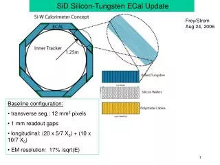
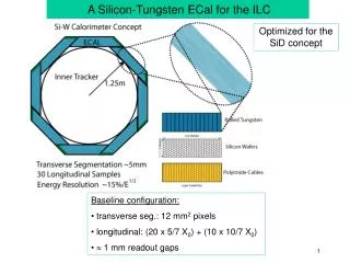
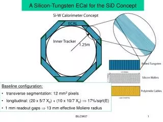
A Silicon-Tungsten ECal for the SiD Concept. Baseline configuration: transverse segmentation: 12 mm 2 pixels longitudinal: (20 x 5/7 X 0 ) + (10 x 10/7 X 0 ) 17%/sqrt(E) 1 mm readout gaps 13 mm effective Moliere radius. “U.S.” Si-W ECal R&D Collaboration. KPiX readout chip

E N D
A Silicon-Tungsten ECal for the SiD Concept • Baseline configuration: • transverse segmentation: 12 mm2 pixels • longitudinal: (20 x 5/7 X0) + (10 x 10/7 X0) 17%/sqrt(E) • 1 mm readout gaps 13 mm effective Moliere radius BILCW07
“U.S.” Si-W ECal R&D Collaboration • KPiX readout chip • downstream readout • detector, cable development • mechanical design and integration • detector development • readout electronics • readout electronics • cable development • bump bonding • mechanical design and integration M. Breidenbach, D. Freytag, N. Graf, G. Haller, R. Herbst, J. Jaros Stanford Linear Accelerator Center J. Brau, R. Frey, D. Strom, M. Robinson, A.Tubman U. Oregon V. Radeka Brookhaven National Lab B. Holbrook, R. Lander, M. Tripathi UC Davis Y.Karyotakis LAPP Annecy BILCW07
Goal of this R&D Design a practical ECal which (1) meets (or exceeds) the physics requirements (2) with a technology that would actually work at the ILC. • The physics case implies a highly segmented “imaging calorimeter” with modest EM energy resolution Si-W • The key to making this practical is a highly integrated electronic readout: • readout channel count = pixel count / 1000 • requires low power budget (passive cooling) • must handle the large dynamic range of energy depositions (few thousand) with excellent S/N • This takes some time to develop (getting close). • Testing in beams will be crucial (major test in 2008). BILCW07
“Imaging Calorimeters” A highly segmented ECal is an integral part of the overall detector particle reconstruction and tracking (charged and neutrals) o in SiD BILCW07
Segmentation requirement • In general, we wish to resolve individual photons in jets, tau decays, etc. • The resolving power depends on Moliere radius and segmentation. • We want segmentation significantly smaller than Rm Two EM-shower separability in LEP data with the OPAL Si-W LumCal (David Strom) BILCW07
Silicon detector layout and segmentation • Silicon is easily segmented • KPiX readout chip is designed for 12 mm2 pixels (1024 pixels for 6 inch wafer) • Cost nearly independent of seg. • Limit on seg. from chip power (2 mm2 ) (KPiX) Fully functional prototype (Hamamatsu)
EM Energy Resolution • Requirement for jet energy resolution in PFAs is modest for EM: 0.20/sqrt(E) • There is no known strong physics argument for excellent EM energy resolution. Our current design provides moderate resolution: 0.17/sqrt(E) However, it is useful to know how to “dial in” different resolutions, if needed. Lines of constant resolution 1 GeV photons Dependence on Si thickness due to straggling. BILCW07
Tungsten Tungsten US Si-W readout gap schematic cross section Metallization on detector from KPix to cable Bump Bonds Kapton Data (digital) Cable KPix Si Detector Kapton Heat Flow Thermal conduction adhesive Gap 1 mm BILCW07
“Longitudinal” Data Cable “Transverse” Data Cable Data Concentrator Conceptual Schematic – Not to any scale!!! Locating Pins Readout Chip “KPix” Detectors Tungsten Radiator ~ 1m BILCW07
KPiX chip One channel of 1024 Dynamic gain select 13 bit A/D Si pixel Storage until end of train. Pipeline depth presently is 4 Leakage current subtraction Event trigger calibration BILCW07
KPiX Cell 1 of 1024 • 64-channel prototypes: • v1 delivered March 2006 • v4 delivered Jan 16, 2007 • It’s a complicated beast – may need a v5 before going to the full 1024-channel chip ? BILCW07
Dynamic Range KPiX-2 prototype on the test bench 1 MIP (4 fC) Max signal: 500 GeV electron BILCW07
Power Pulsing • Switch off KPiX analog front-end power between bunch trains (1% duty cycle) • Average power of 18 mW per channel • passive-only cooling should be OK BILCW07
prototype Si detector studies BILCW07
v2 Si detector – for full-depth test module • 6 inch wafer • 1024 12 mm2 pixels Allows for topside bias Vertices removed for spacers Trace layout minimizes Cmax Uses thinner traces near KPiX Low resistance power and ground connections ready to go except for funding BILCW07
R&D Milestones • Connect (bump bond) prototype KPiX to prototype detector with associated readout cables, etc • Would benefit from test beam (SLAC?) - 2007 • A “technical” test • Fabricate a full-depth ECal module with detectors and KPiX-1024 readout * – functionally equivalent to the real detector • Determine EM response in test beam – 2008 • Ideally a clean 1-30 GeV electron beam (SLAC?) • Test with an HCal module in hadron test beam (FNAL?) – 2008-? • Test/calibrate the hadron shower simulations; measure response • Pre-assembly tests of actual ECal modules in beam – >2010 BILCW07 pending funding
Summary • The R&D leading to an “ILC-ready” Si-W ECal technology is progressing well. • There are no show-stoppers for meeting the demanding physics and technical requirements. • This effort depends crucially on highly integrated readout electronics (KPiX) • This Si-W R&D should result in full-depth modules which will require test beam evaluation • Our Si-W module (30 layers x 16cm x 16cm) - 2008* • These highly segmented, analog devices should provide an interesting test for simulation modeling of (early developing) hadron showers. BILCW07