Crystal Structure & Wafer Fabrication in Silicon Technology
420 likes | 715 Views
Learn about single crystal, polycrystalline, and amorphous structures in silicon technology, the importance of single crystal silicon in semiconductor devices, and crystallography concepts. Explore the properties and applications of different crystal structures in wafer fabrication processes.

Crystal Structure & Wafer Fabrication in Silicon Technology
E N D
Presentation Transcript
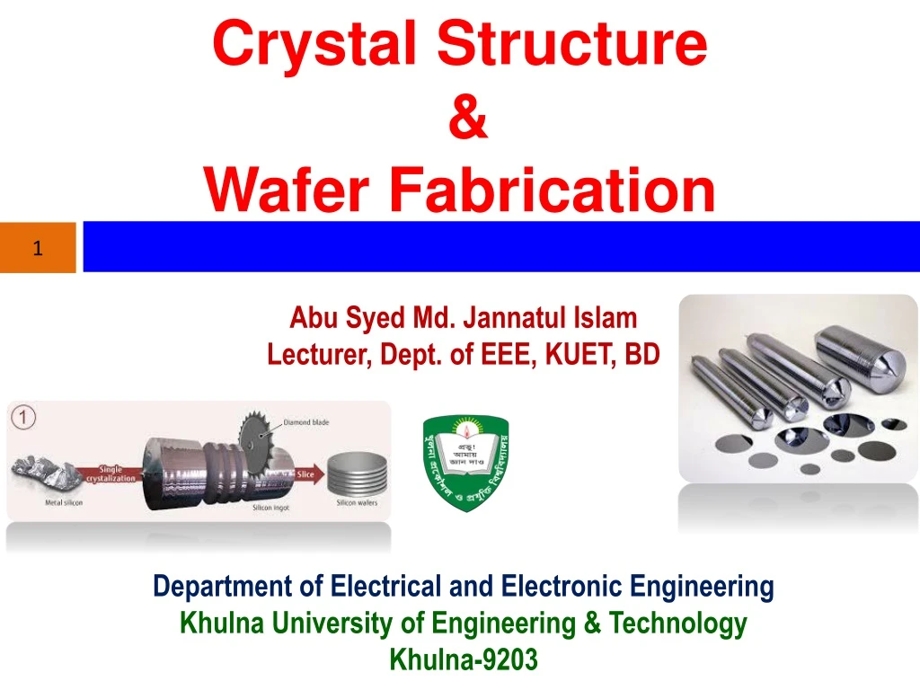
Crystal Structure &Wafer Fabrication 1 • Abu Syed Md. JannatulIslam • Lecturer, Dept. of EEE, KUET, BD • Department of Electrical and Electronic Engineering • Khulna University of Engineering & Technology • Khulna-9203
Crystal 3 Single crystal Polycrystalline Amorphous Liquid crystal
Insulin crystals Gallium, a metal that easily forms large single crystals Single Crystal 3 A single crystal/mono-crystal, is a crystalline solid in which the crystal lattice of the entire sample is continuous and unbroken to the edges of the sample, with no grain boundaries. Mono/single Si serves aslight-absorbing material in the manufacture of solar cells. Quartz crystal Silicon
Polycrystalline 3 • Polycrystalline materials are solids that are composed of many crystallites of varying size and orientation. • The crystallites are referred to as grains. • The variation in direction can be random (called random texture) or directed, possibly due to growth and processing conditions. • Fiber texture is an example of the latter. Almost all common metals, and many ceramics are polycrystalline.
Amorphous Solid 3 • An amorphous solid is a solid in which there is no long-range order of the positions of the atoms • Most classes of solid materials can be found or prepared in an amorphous form. • For instance, common window glass is an amorphous ceramic, many polymers (such as polystyrene) are amorphous, and even foods such as cotton candy are amorphous solids. • The amorphous structure of glassy Silica (SiO2). • No long range order is present, however there is local ordering with respect to the tetrahedral arrangement of Oxygen (O) atoms around the Silicon (Si) atoms.
Silicon 3 • Si and atomic number 14 14. The atomic mass is 28.0855. • Silicon, like carbon and other group IV elements form face-centered diamond cubic crystal structure. • Silicon, in particular, forms a face-centered cubic structure with a lattice spacing of 5.430710 A (0.5430710 nm).
Why Silicon? 16 Silicon is abundant in the earth crest as an ore in the form of quartzite and it is a low cost material. Other reason: It forms an oxide that is of very high quality, seals the surface with very few pin holes or gaps. This allows gap MOSFET to be more easily made as the SiO2 forms the insulating layer for the Gate, Protects and passivatesunderlying circuitry helps in patterning and useful for dopant masking. It forms a very tough Nitride- Si3N4(Silicon Nitride) forms a very high band gap insulator which is impermeable. This is used to passivate (seal) the die. This also used to make hard masks and in other process steps Si has a very nice bandgap of ~ 1.12 eV, not too high so that room temperature can't ionize it, and not so low that it has to high leakage current.
Why Silicon? 17 • Silicon has relatively high dielectric strength and therefore is suitable for power devices. • It forms a very nice gate material. Most modern FET's used in VLSI (up until the latest generations) have been called MOSFET but in actual fact have used Si as the gate material. • Stable and strong material & crystal structure like diamond • Higher operating temperature (125-175ºC vs. ~85 ºC) and thus become intrinsic at higher temp. • Large variety of process steps possible without the problem of decomposition (as in the case of compound semiconductors) • GeO2 - is partially soluble • GaAs - does not form a oxide • CO2 - is a gas • Recently, SiC becoming popular due to high temperature tolerance and high power, high frequency operation. …
Why Silicon? 18 Crystal structure : diamond cubic Magnetic ordering: diamagnetic Electric resistivity : (20 °C) 103Ω·m Thermal conductivity: (300 K) 149 W·m−1·K−1 Thermal expansion : (25 °C) 2.6 µm·m−1·K−1 Speed of sound : (thin rod) (20 °C) 8433 m/s Young’s modulus: 185 GPa Shear modulus : 52 GPa Bulk modulus :100 GPa Band gap energy at 300 K : 1.12eV
Importance of Single Crystal Silicon 3 • Semiconductor devices and VLSI (very large scale integrated) circuits require high-purity single-crystal semiconductors. Because: • Difficult to control properties of amorphous or poly-crystals. • By doping, electronic properties (carrier density, mobility, conductivity, carrier lifetime) of a single crystal can be controlled more precisely. • Amorphous silicon is used in photovoltaic cells, electronic displays (large-area). • Polycrystalline silicon is used as a gate contact in MOSFETs (VLSI circuits). Single crystal Si wafers Diameters: currently up to 300mm (500mm?) Wafer thickness: 650μm Wafer purity: 150 parts/trillion Impurities: 99.99999999% Si
Crystallography 3 • Crystals are characterized by a unit cell which repeats in the x, y, z directions. • Planes and directions are defined using an x, y, z coordinate system. • [111] direction is defined by a vector having components of 1 unit in x, y and z. • Planes are defined by Miller indices - reciprocals of the intercepts of the plane with the x, y and z axes.
Silicon Wafer Manufacturing 3 • CzochralskiMethod • Float Zone Method • Bridgman Method
Metallurgical Grade Silicon 3 Quartzite (sand, SiO2) is placed in a hot (1800oC) furnace with carbon releasing materials, and reacts as shown, forming metallurgic grade silicon (MGS): 2SiO2(solid) + 2C(solid) Si(liquid) + 2CO(gas) Metallurgical grade silicon (~98% pure) production and typical impurity levels. Over 50% MGS is used to make Al alloys. The fraction used for semiconductors is very small.
Electrical Grade Silicon (polycrystalline) 3 • Basically, the solid Si is first converted into a liquid form (SiHCl3) for purification, then converted back into solid Si. • Both reactions occur at high temperatures. • Metallurgical grade silicon is treated with hydrogen chloride to form tri-chlorosilane: • Si + 3HCl SiHCl3(g) + H2(g) (use catalyst) • SiHCl3 is liquid at room temperature, boiling point 32oC. Multiple distillation of the liquid removes the unwanted impurities (99.9999% pure). • The purified SiHCl3 is then used in a hydrogen reduction reaction to prepare the electronic grade Si (EGS): • SiHCl3(g) + H2(g) Si(s) + 3HCl(g) • (this is the reverse reaction of the above reaction) • EGS is the raw material for Si single crystal production.
CzochralskiMethod 3 Jan Czochralski (1885 - 1953) was a Polish chemist who invented the Czochralski process, which is used to grow single crystals and is used in the production of semiconductor wafers. He discovered the Czochralski method in 1916 when he accidentally dipped his pen into a crucible of molten tin rather than his inkwell. He immediately pulled his pen out to discover that a thin thread of solidified metal was hanging from the nib. The nib was replaced by a capillary, and Czochralski verified that the crystallized metal was a single crystal.
Czochralski Method 3 • It is widely employed for Si, GaAs, and InP. • The EGS is broken into small pieces and placed in an SiO2crucible. • In an argon ambient, the crucible is heated to just above 1417oC. • Dopant is added to the melt to intentionally dope the resulting crystal. • A single crystal seed is then lowered into the melt (crystal orientation and wafer diameter determined by seed orientation and pull rate), and withdrawn slowly.
Czochralski Method 3 • Melt flows up the seed and cools as crystal begins to grow. • Seed rotated about its axis to produce a circular cross-section crystal. The rotation inhibits the natural tendency of the crystal to grow along certain orientations to produce a faceted crystal. • Long ingots (boules) 100 kg, with very good circular cross-section are produced. • The oxygen and carbon (from graphite furnace components), contribute about 1017-1018/cm3 contaminants.
Czochralski Method 3 A commercial CZ puller Early in the growth process Later in the growth process
Oxygen and Carbon in CZ silicon 3 • The CZ growth process inherently introduces O (from SiO2 crucible) and C (from graphite susceptor/supporter). • Typically, CO ≈ 1018 cm-3 and CC ≈ 1016 cm-3. • The O in CZ silicon often forms small SiO2 precipitates in the Si crystal under normal processing conditions. • O and these precipitates can actually be very useful: provide mechanical strength, internal gettering.
Dopant Incorporation 3 • Dopants are added to the melt to provide a controlled N or P doping level in the wafers. • However, the dopant incorporation process is complicated by dopant segregation. • Generally, impurities “prefer to stay in the liquid” as opposed to being incorporated into the solid. • This process is known as segregation. The degree of segregation is characterized by the segregation coefficient, ko, for the impurity. CS CL CS and CL are the impurity concentration just on the either side of the solid/liquid interface.
Dopant behavior during crystal growth 3 Most k0 values are <1 which means the impurity prefers to stay in the liquid. Thus as the crystal is pulled, dopant concentration will increase. In other words, the distribution of dopant along the ingot will be graded.
Preparing crystal ingot for grinding • Diameter grind • Flat grind Ingot Grinding 3
Ingot Grinding 3 • This means first precisely aligning the crystals, then cylindrical grinding of the ingot pieces to the required diameter. • The final step is grinding orientation markings, such as notches for large-diameter wafers or straight edges (flats) on the side of small wafers.
Wafer Slicing 3 • The first step when wafering the silicon ingots is multi-wire slicing, which is the slicing method commonly employed today. • A very thin metal wire, which can be many miles long, is pulled over the wire guide rollers in such a way that a wire web with very precise spacing is spanned. • Nozzles apply the slurry to the web while the silicon ingot is slowly pushed through the web. This technology makes it possible to slice complete silicon ingots into hundreds of silicon wafers in just one step. • The individual process parameters must be carefully monitored in order to guarantee that the wafers are uniformly thick and that the two faces of each wafer are parallel to each another. • After slicing, edge rounding, mechanical lapping and wet chemical etching is performed before final chemical mechanical polishing. The wet etching is typically: • 3Si + 4HNO3 + 18HF 3H2SiF6 + 4NO + 8H2O
Edge Rounding 3 • Monocrystalline silicon is a very brittle material with a high risk of breaking. • Special care is consequently needed in order to avoid mechanical damages on the edge of the wafer. • The unrounded silicon wafer is mounted onto a grinding chuck and a profile rounding wheel rounds the edge of the wafer. • The edge profile is rounded to match the customer specifications. • Each wafer is optimized in order to avoid processing damages and maximize the yields in the component processes, such as CMP and lithography.
Laser Marking 3 • Laser marking is used to identify individual wafers or wafer batches in order to allow manufacturing traceability. • Laser marking can take place in accordance with either industry standard or customer specifications. As a rule, the markings contain information on the wafer supplier, some technical information, and an individual wafer number.
Wafer Lapping 3 • After the wafers have been sliced and the edges have been rounded, the wafers are lapped (or alternatively ground) in order to increase the parallelism of the silicon wafer surfaces and to remove any damage below the surface caused by the slicing process. • For lapping, the silicon wafers are held in carrier wheels (lapping carriers) between the upper and lower lapping plates, which rotate in opposite directions. The addition of an abrasive (lapping slurry) helps remove roughly ten micrometers of silicon from each wafer surface.
Wafer Etching and Cleaning 3 • the silicon wafers are etched and cleaned in order to eliminate any remaining mechanical damage. Alkaline solutions, acids, or a combination of the two can be used for the etching.
Wafer Polishing 3 Chemical mechanical polishing • Polishing makes the silicon wafer surface smooth as glass and further improves the flatness. • The wafers are mounted on support plates and pressed against a polishing cloth that lies on a polishing plate. • Wafers with a diameter of 200mm or less are usually polished on one side. • Wafers with a diameter of 300mm are polished on both sides. • Like in the lapping process, the wafers are held by plates and simultaneously polished on the front and back by upper and lower polishing plates. • The polishing agent (polishing slurry) and the pressure scheme determine the finished wafer’s surface quality and flatness.
Advantage of larger diameter wafers 3 More chips per wafer for larger wafer.
Crystal Growth • Wafer Lapping and Edge Grind by Al2O3 and glycerine • Cleaning • Remove seed and • Other end of ingot • Etching for removing surface damage • Inspection • Polishing • Packaging • Wafer Slicing by diamond saw Steps for Wafer Preparation 3 • Grinding to special diameter and ground some flat region