Download
1 / 23
250 likes | 510 Views
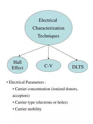
Electrical Techniques . MSN506 notes. Electrical characterization. Electronic properties of materials are closely related to the structure of the material on the atomic scale In order to use materials in device applications, we must characterize and understand their electrical properties

E N D
Electrical Techniques MSN506 notes
Electrical characterization • Electronic properties of materials are closely related to the structure of the material on the atomic scale • In order to use materials in device applications, we must characterize and understand their electrical properties • Study of electrical properties at the nanometer scale is in itself interesting to physics, as quantum effects may dominate in this regime, even at room temperature
Conduction regimes • Bulk macroscopic conduction • Large number of states contribute to overall current • Large number of electrons • Resistivity, mobility, electric field, bias voltage, macrocopic currents • Metals, semiconductors, polymeric conductors • Quantum effects are averaged out by thermal effects
Conduction at the nanoscale • Small number of states can affect the overall current • Wavefunction coherence lengths are comparable to characteristic device dimensions • Single electrons charging effects can be significant • These can amount to overall macroscopic electronic properties that show deviations from bulk electronic properties http://www.nanohub.org/courses/fundamentals_of_nanoelectronics
Charge transport • Convenient simplifications to reduce complexity of problem • Still can be quite complicated • Drift-Diffusion • Bulk-like transport in semiconductors • Bolztman Transport Equation • Semiclassical transport considering the distributions of carriers to energies and momenta, taking into account scatterings • Tunneling picture
Flow of electrons between two reservoirs • Electrons obey the Fermi-Dirac distribution A metal/semiconductor electrode Two electrodes with some other material (states) in between As T ~ 0 K, this becomes a step function
Flow of electrons between two reservoirs Two electrodes with some other material (states) in between Availability of carrierson the left, and empty slots on the right, How fast the carriers tunnel from the left to the center How fast the carriers tunnel from the center to the right … basically determine the current
Transconductance Amplifier • Converts the current into a voltage
Low temperature Preamplifier • Opamps can not be cooled • An FET preamplifier can help carry the signal to a room temperature stage
IV spectroscopy • Measuring IV as a function of • Temperature • Illumination • Magnetic field etc. • Gives information about • the material conductivity, band structure, carrier concentration • Contacts • Transport mode
Probe Station • Multiple probes can be used to make IV and other electrical measurements on micofabricated devices
Four point technique • Make quick measurements of conductivity on novel materials where contacts are not ideal t >> s Bulk Sample Thin Sheet thickness t << s Typical probe spacing s ~ 1 mm
Capacitance Measurements • Parallel plate capacitor Linear capacitor Parallel plate We can measure dielectric constant if we know the dielectric thickness
Capacitance Spectroscopy • When • semiconductors are used (surface potential and electric field are not linearly dependent) • the dielectric layer has electric field dependent conductivity (loss) • There are traps (or states) that can be charged and discharged only at certain voltages • We can measure the small signal capacitance as a function of DC bias, and interpret C-V curves to gain information about the system
C-V characterization of MOS structures • Measurement of C-V characteristics • Apply any dc bias, and superimpose a small (15 mV) ac signal • Generally measured at 1 MHz (high frequency) or at variable frequencies between 1KHz to 1 MHz • The dc bias VG is slowly varied to get quasi-continuous C-V characteristics
Measured C-V characteristics on an n-type Si ND = 9.0 1014 cm3 xox = 0.119 m
Doping dependence of a MOS capacitor Can tell you carrier concentration, dielectric thickness or constant, Dielectric interface trap densities, Carrier diffusion properties etc.
Capacitance Measurements • Modelling can help you extract many material properties
Capacitance Measurements • Example: Quantum states of InAs nanostructures in GaAs
Capacitance Measurements • Example: Quantum states of InAs nanostructures in GaAs
DLTS: Deep Level Transient Spectroscopy • Measures escape rate of carriers