Download
1 / 24
270 likes | 532 Views
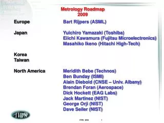
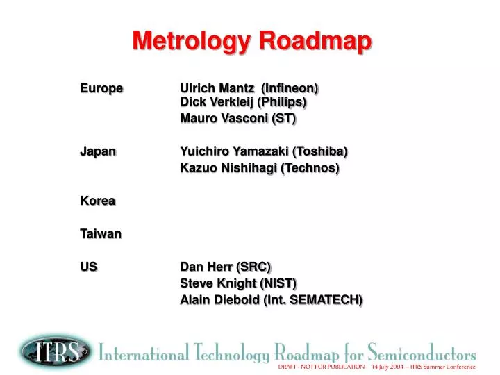
Metrology Roadmap. Europe Ulrich Mantz (Infineon) Dick Verkleij (Philips) Mauro Vasconi (ST) Japan Yuichiro Yamazaki (Toshiba) Kazuo Nishihagi (Technos) Korea Taiwan US Dan Herr (SRC) Steve Knight (NIST) Alain Diebold (Int. SEMATECH). Metrology Roadmap 7/12/04.

E N D
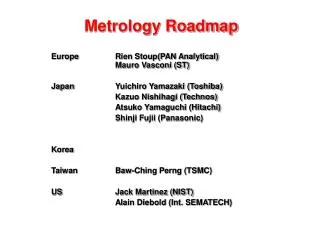
Metrology Roadmap Europe Ulrich Mantz (Infineon) Dick Verkleij (Philips) Mauro Vasconi (ST) Japan Yuichiro Yamazaki (Toshiba) Kazuo Nishihagi (Technos) Korea Taiwan US Dan Herr (SRC) Steve Knight (NIST) Alain Diebold (Int. SEMATECH)
Metrology Roadmap7/12/04 Japan Yuichiro Yamazaki (Toshiba) US Dan Herr (SRC) Steve Knight (NIST) Alain Diebold (Int. SEMATECH) Dan Wack (KLA-Tencor) Wen-Li Wu (NIST) John Allgair (Freescale/ISMT) Andras Vladar (NIST) Vladimir Ukraintsev (Texas Instruments) Michael Gostein (Philips AMS) Mike Haina (KLA-Tencor) Rick Silver (NIST) Ben Bunday (ISMT)
AGENDA • 2004 ITRS Changes and Activities • Lithography Metrology • FEP Metrology • Interconnect Metrology • Key Challenges
New Business • Established link with Emerging Research Materials group of ERD • ERM to report requirements • Metrology Reports Methods and Discussion • Provided update on aberration corrected TEM and 3D TEM developments • Awaiting changes in Process Tolerance for Gate CD
Metrology Critical Challenges Five Difficult Challenges ³ 45 nm, Through 2009 • Metrology Integration • Starting Materials and In-line Metrology for strained Si, SiGe, and SOI • Control of high-aspect ratio technologies including copper void detection • Measurement of complex material stacks and interfacial properties • Measurement test structures and reference materials
Metrology Critical Challenges Five Difficult Challenges < 45 nm, Beyond 2009 • Nondestructive, production worthy, wafer and mask level microscopy for CD and overlay • New strategy for in-die metrology must reflect across chip and across wafer variation • Statistical limits of sub-45 nm process control • Structural and elemental analysis at device dimensions. i.e. materials characterization • Development of manufacturing metrology when device and interconnect technology remain undefined
2004 ITRS Activities • Update all Technology Requirements Tables • Initiate new work for 2005 Rewrite • Look at Litho CD Potential Solutions • Expand Overlay Section • Expand discussion of new areas such as SEM overlay • Look at new areas of FEP activity • Local Stress Measurements • Metal Gates • Look at Interconnect long term needs
Changes to Litho CD Metrology ITRS July Presentation by Dan Wack – KLA-Tencor Scatterometry to at least the 45 nm Node Bryan Rice (Intel), SPIE, 2004 CD-SEM and Scatterometry can reach 32 nm Node w/improvement – impact of SOI not tested 45 nm contact Holes 16 nm Lines -176 nm Pitch
Recommended New Wording for LWR and re-instating LER metric • This is the new wording for consideration: “The LWR metric used in this document is defined to be 3 times the standard deviation of the CD, sampled so as to include all (and only) those roughness wavelengths between λmin and λmax” • λmin and λmax are dependent on the node, and both needed to be specified
Overlay Metrology • Issues are with the Overlay Targets • Need better correlation between overlay target and device performance • Current roadmap suggests that overlay is in good shape because precision for box – in – box targets meets ITRS guidelines • Step and Scan Litho Exposure tools contribute errors not measured by scribe line targets • Across die overlay issues are not captured by box –in – box target data analysis • 2005 rewrite will capture these issues
w 2q 2004 Potential Solution Assessments • Conflicting Reports on high keV CD-SEM Damage • Impact of Metal Gate on CD-SEM and Scatterometry – Metal Dependent • Impact of Gate thickness on CD Measurement for end of roadmap • New Method identified as potential solution – CD-SAXS (NIST Wen-Li Wu)
FEP : High Metrology • Metal Gate & high both require metrology development • Stress Measurement • SOI and Strained Silicon • New Transistor Designs
Increasing Emphasis on Areas beyond High k • Increase in Mobility by using local stressing of transistors – Call for stress metrology by FEP • Metal Gates increasingly important • New transistor designs are already past R and into D. Example: FIN-FETs require metrology • Strained SOI, GeOI considered longer term substrates • Crystal Defect mapping including on patterned wafers metrology requirement for new substrates • Mobility measurements are key
90 nm node High Volume CMOSStrained Si substrates not used PMOS Compressive Strain increased hole mobility 45 nm NMOS Tensile Stress SiN Layer increased electron mobility From T. Ghani, et. al., IEDM 2003, p 978. Courtesy Intel
Gaps in Interconnect Metrology • VOID Detection in Copper vias & lines now based on 1/10 via diameter • Quality of Barrier/Seed on sidewalls& low trench/via sidewalls • Killer Pore Detection in Low kpore size distribution • Non destructive metrology for adhesion and (eff) (at operating freq.) for patterned wafers
2004 Interconnect Activities • Porous low k is being overshadowed by the need to lower k value of barrier layer and etch stops for 45/32 nm node. • Long term solution for interconnect is ambiguous.
New Comments on Interconnect Metrology • 3D CD especially Sidewall Roughness for trench/via are critical needs • In Process Development, LER is an important figure of merit for sidewall and AFM can give sidewall/via roughness vs depth as well as trench CD and profiles which provide important control for etch processes • Need metrology for thickness and uniformity for hard mask above low after CMP – how is erosion pattern dependent
ERD and ERMPremise: Aberration corrected TEM/STEM needed for nano-electronics • Latest TEM and STEM results show improved imaging for sub 0.1 nm beams. • We have not reached the limit where improving beam diameter does not improve imaging • Nanowires and nanotubes serve as ideal systems to test theoretical and experimental understanding of beam propagation and image formation. - reduced stresses and amorphous films on the surface
Concept Proven : Aberration Correction STEM – Batson, Dellby, and Krivanek, Nature 418, 617 (2002) Si(110) HR-TEM – Jai, Lentzen, and Urban, Microsc. Microanal. 10, 174, 2004. SrTiO3 Before After
Conclusions • CD Measurement improvements show a path to the 32 nm Node • Propose definition for LWR and including LER • Transistor channel engineering requires Stress and Mobility Measurement • Interconnect requires Sidewall Measurements for barrier/seed and low trench
Acknowledgements • David Bell and his 2003 M&M paper on nanowire TEM • Christian Kiselowski • Dave Muller • Steve Pennycook • Suzanne Stemmer