Metrology Roadmap 2010
Metrology Roadmap 2010. Europe Adrian Kiermasz (Metryx) Carlos Beitia ( CEA LETI MINATEC ) Philippe Maillot (ST) Delphine Le Cunff (ST) Japan Yuichiro Yamazaki (Toshiba) Masahiko Ikeno (Hitachi High-Tech) Korea Taiwan North America Yaw Obeng (NIST)

Metrology Roadmap 2010
E N D
Presentation Transcript
Metrology Roadmap2010 Europe Adrian Kiermasz (Metryx) Carlos Beitia (CEA LETI MINATEC) Philippe Maillot (ST) Delphine Le Cunff (ST) Japan Yuichiro Yamazaki (Toshiba) Masahiko Ikeno (Hitachi High-Tech) Korea Taiwan North America Yaw Obeng (NIST) George Orji (NIST) Jack Martinez (NIST) Dave Seiler (NIST) Ben Bunday (ISMI) Vic Vartanian (ISMI) Alain Diebold (CNSE – Univ. Albany)
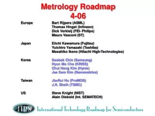
200K 20K 2K Metrology/Char. Research Tool Metrology Beta Tool w/precision Metrology Product Tool w/prec. & Uncert. Metrology Alpha Tool 200 20 First Tech. Conf. Device Papers Up to ~12yrs Prior to Product 2 0 24 -96 -72 -24 -48 Metrology Timing Model w/Technology Cycle Timing New for 2010 Production Research Development Process Research Tool Alpha Tool Beta Tool Product Tool Volume (Wafers/Month) 1st 2 Co’s Reach Product First Tech. Conf. Circuits Papers Up to ~ 5yrs Prior to Product Months 2011 2013 2015 2017 2019 2021 Source: 2009 ITRS - Executive Summary Fig 2b
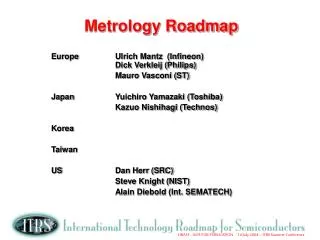
200K 20K 2K 200 20 First Tech. Conf. Device Papers Up to ~12yrs Prior to Product 2 0 24 -96 -72 -24 -48 Metrology Materials and Test Structure Timing Model w/Technology Cycle Timing New for 2010 Production Research Development Metrology Research Tool Metrology Beta Tool w/precision Metrology Product Tool w/prec. & Uncert. Metrology Alpha Tool Metrology Research Samples Metrology Test Structure Samples @ Man. Design Rules Volume (Wafers/Month) 1st 2 Co’s Reach Product First Tech. Conf. Circuits Papers Up to ~ 5yrs Prior to Product Months 2011 2013 2015 2017 2019 2021 Source: 2009 ITRS - Executive Summary Fig 2b
Litho Metrology Spacers CD-SAXS Contour vs Design Dual Patterning LER CD Metrology Extendibility MuGFET MuCFET Litho Metrology for 3D Devices Muller Matrix Ellipsometry
+ III/V High µAlternative Channel Mat’ls Metrology for FEP EOT & Defects for Alternate Channel Materials Metrology for Generation II and III High K stacks Sidewall Metrology for 3D Devices MuGFET MuCFET FDSOI Nano-topography & Local Stress measurements • New Memory Materials • Phase Change Memory
Metrology for ERM/ERD High carrier mobility and structural robustness have driven a considerable effort in Graphene research Measurement of Bi-layer misorientation Aberration corrected TEM How many Layers? Raman and LEEM Quantum Hall Effect observes the Berry Phase
Metrology for 3D Interconnect Overlay – IR Microscopy X-Ray Microscopy 4 3 1 Bonding Defects - SAM Stress Metrology Raman Microscopy F)
Metrology Summary 3D Metrology for Advanced Memory • FEP-Interconnect-Litho • PC and SST RAM - New materials for Metrology • Dual Patterning • 3D Metrology – Confirm Geometry Requirements e.g. film thickness & properties on sidewall • Reference Methods for 3D • Composition & Stress – e.g. buried channels • EUV metrology requirements • ERD-ERM • III-V & Ge Transition to FEP & PIDS • STT RAM Transition to FEP & PIDS • Tunnel Dielectric • Magnetic layers and interfaces • Redox RAM • Local characterization of oxygen vacancies • Real device dimensions and structures • Deterministic Doping • Characterize dopants in 3D • Dopant vacancies and interstitials • Directed Self Assembly • Defect detection • Structure variations • Graphene • Defects in CVD Graphene • Mobility & Substrate Interactions • Bandgap Measurement (Strain, etc.) Graphene – C. Kisielowski