Download

1 / 46
460 likes | 694 Views
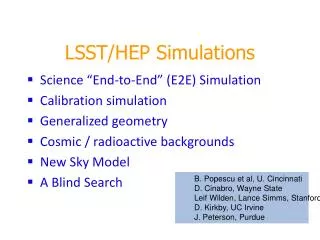
Activités Microélectroniques sur LSST. Hervé Lebbolo pour le groupe LSST électronique LAL / LPNHE. LSST : Large Synoptic survey Telescope. Telescope and site : Cerro Pachon , Chile. Temps de pose : 15s Lecture : 2s. 4 cm. Plan focal & Rafts. RSA. 4K x 4K CCD 10mm pixels = 0.2”

E N D
Activités Microélectroniques sur LSST Hervé Lebbolo pour le groupe LSST électronique LAL / LPNHE Hervé Lebbolo - Journées VLSI - Lyon - 07/06/2012
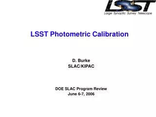
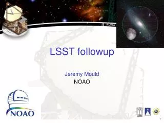
LSST : Large SynopticsurveyTelescope Telescope and site : Cerro Pachon, Chile Temps de pose : 15s Lecture : 2s Hervé Lebbolo - Journées VLSI - Lyon - 07/06/2012
4 cm Plan focal & Rafts RSA • 4K x 4K CCD • 10mm pixels = 0.2” • extended red response • 16 outputs • 5mm flatness CRYOSTAT FEC RCC • RAFT • 9 CCDs • coplanarity 13.5mm • 92% fill factor • TOWER • CCDs + front end electronics • 180K operation • An autonomous, fully-testable and serviceable 144 Mpixel camera 21 rafts, with 9 CCDs each CCD : 16 * 1Mpixel Camera : ~3Gpixel Hervé Lebbolo - Journées VLSI - Lyon - 07/06/2012
Chaîne de lecture de la caméra RCM CABAC 18 bit ADC ASPIC : Analogue Signal ProcessingIntegated Circuit CABAC : Clocks And BiasesAsic for CCD Readout : 500kHz Hervé Lebbolo - Journées VLSI - Lyon - 07/06/2012
ASPICRequirements • 8 channels dual slope integrator • Operates @ 173K • CCD readout @ 550kHz– up to 1MHz • Power dissipation : 25mW / channel • Power Supply 0/5V with respect to reference = 2.5 V • Noise : • ~5nV / √Hzmaximum noise density [ 5 to 6 e- read noise (10nV/ √ Hz) for the whole CCD chain] • 7µVrms for 500ns integration [<2 e-] • Crosstalk : 10-4level[ 0.01% (goal) - 0.05% (max) ] • Full Well capacity : • 90keˉ [150keˉ max] ie~400mV max input • Linearity : 0.5%[defined over to full well scale] • Differential outputs • Output Load : 50pF // 1 k Ω • Nap mode Hervé Lebbolo - Journées VLSI - Lyon - 07/06/2012
Read Out Method : Dual Slope Integration CCD Reset CCD Output ASPIC Reset ADC S/H Ramp Down (integrate noise) Ramp Up (integrate signal + noise) One of the 2 differential channel output Integration Time Tint Isolation Time Dual SlopeIntegrationsequence Hervé Lebbolo - Journées VLSI - Lyon - 07/06/2012
ASPIC (2) Input amp • 3 programmable input amplifier gains :2.5 – 5 – 7.5 • to deal with CCD gain spread. • 3 integration time constants : 500ns – 1µs – 1.5µs • to deal with CCD readout frequency. baseline : {gain 5 & 500ns integration time} Hervé Lebbolo - Journées VLSI - Lyon - 07/06/2012
Schéma de Base Hervé Lebbolo - Journées VLSI - Lyon - 07/06/2012
ASPIC 2 layout • Techno : CMOS 0.35µ 5V • Vendor: AMS • Package 1 : CQFP100 • Package 2 : QFN100 avec bottom pad pour un meilleur contact thermique • Surface : 2,7*3,8 mm² Hervé Lebbolo - Journées VLSI - Lyon - 07/06/2012
ASPIC2 tests bench Programmable Power Supplies ASPIC (2) Front End Board (cryo or room temperature) Custom Back End Board (8*18 bit ADC Altera FPGA) PC + LabView Switches Board ck 127dB / 1dB step Programmmable attenuator generators signal Hervé Lebbolo - Journées VLSI - Lyon - 07/06/2012
Back End Board Output to CCD USB FIFO FPGA Gain switches External trigger Output to ASPIC : clocks, commands ADC channel Input (from ASPIC) Hervé Lebbolo - Journées VLSI - Lyon - 07/06/2012
Cold Front end (LPNHE) Outputs and power supply Clocks and settings Inputs Cooling: front-end card connected to nitrogen circuit 4 CCD inputs Temperature sensors & heating Flex cable and 37-pin connector (17 grounded) Shielding with thermal break (mesh) Hervé Lebbolo - Journées VLSI - Lyon - 07/06/2012
LAL Cold Test Stand QFN Packaging Withbottom pad 8 input Clamp for X talk measurements Sub Micro D connectors Hervé Lebbolo - Journées VLSI - Lyon - 07/06/2012
ASPIC II Measurements : Gain • Chip-to-chip rmsdispersion = 2% • In-chip dispersion rms dispersion = 0.3% on average – 0.5% atmost Gain measured over 37 chips *: R&C extraction Hervé Lebbolo - Journées VLSI - Lyon - 07/06/2012
ASPIC II Measurements : Gain Hervé Lebbolo - Journées VLSI - Lyon - 07/06/2012
ASPIC II Measurements : Noise Effect of input amplifier bias le bruit peutêtre encore diminuési le budget puissance augmente Hervé Lebbolo - Journées VLSI - Lyon - 07/06/2012
ASPIC 2 Linéarité gain=5 (6), RC=500ns residu: 0.3% gain=2.5 (3.9), RC=500ns residu: 0.4% Requirement : < 0.5 % over full well range Hervé Lebbolo - Journées VLSI - Lyon - 07/06/2012
Measurements : Crosstalk Y axis = source X axis = victim • Xtalkasymetric : injecting a signal in the ch 7 generate more crosstalk than injecting a signal in the ch 0. • When the ASPIC II input stage saturated, the Xtalk also saturates : • Xtalk is probably dependant of the amplitude at the output of the first amplifier. • Notice: • postlayout simulations don’t show any crosstalk effects. • ASPIC I had a smaller Xtalk ( < 0.007 % ) than the ASPIC II and no programmable gain. Hervé Lebbolo - Journées VLSI - Lyon - 07/06/2012
Measurements : Memory Effect of the integrator reset width on the channel memory 150ns 200ns 250ns Hervé Lebbolo - Journées VLSI - Lyon - 07/06/2012
ASPIC2 TESTS DC Asymétrie • Mesure de la réponse à un niveau DC : efficacité de l’annulation du bruit de reset (kT/C) du CCD et de la dérive du signal d’entrée (couplage AC) • Asymétrie : 0,07% ( bruit de reset CCD : 60 e⁻ erreur 0,04 e⁻) • Asymétrie totale ~ asymétrie gains * asymétrie intégration Different gain / Same Time Constant Ramp down Ramp up ASPIC input G+ G- S+ Difference = 0 S- Hervé Lebbolo - Journées VLSI - Lyon - 07/06/2012
ASPIC 2 suite et fin ASPIC 3 • Tests à froid sur long terme : vieillissement ? dégradation des performances ? • Mesures plus fines des effets mémoire, Xtalk, impact des temps d’isolement sur le bruit • Mesures avec le CCD250 ------------------------- • Augmentation du « gain » et du full well (150ke) du CCD d’e2v • diminution du gain (augmentation du bruit) • Programmation plus fine du temps d’intégration et du gain (2*4bit) • Mode transparent (monitoring des signaux CCD) • Sonde de température ? • Programmation par lien série • Amélioration de la vitesse de « réveil » Hervé Lebbolo - Journées VLSI - Lyon - 07/06/2012
ASPIC 3 suite Mode transparent Soumission prévue début 2013 Hervé Lebbolo - Journées VLSI - Lyon - 07/06/2012
CABAC : clockand biasesasic for CCD IΦ3 IΦ0 IΦ1 IΦ2 IΦ3 Fournir les horloges (série et parallèle), les polarisations et les alimentations des amplis de sortie des CCD Hervé Lebbolo - Journées VLSI - Lyon - 07/06/2012
CCD requirements baseline
CABAC requirements • OD and Biases: • 2 OD : 8 bit programmable level from 13 to 36V, 16 mA capability each, exposure & readout levels, load : 100Ω + .1µF • 1 RD : 8 bit programmable level from 13 to 36V, 1kΩ + .1µF load, electronic calibration pulser • 1 GD : 8 bit programmable level from 13 to 36V, 1kΩ + .1µF load • 1 OG : 8 bit programmable level from 0.1 to 4.8V, 1kΩ + .1µF load • 1 spare0 : 8 bit programmable level from 13 to 36V, 1kΩ + .1µF load • 1 spare1 : 8 bit programmable level from 0.1 to 4.8V, 1kΩ + .1µF load • Clocks : • 4 parallel, 8 bit programmable current capability (max 300mA), common voltage rails (ΔV = 20V max), exposure/readout modes (static current divided by 10) • 4 serial, 8 bit programmable current capability (max 16mA), 2 voltage rails (3+1) (max 20V), exposure/readout modes Hervé Lebbolo - Journées VLSI - Lyon - 07/06/2012
CABAC requirements • Readout & Exposure modes input independant from serial programing • Temperature sensor (current source + diode connected mos transistor) • Multiplexor : Possibility to output 2 of any signal provided by CABAC or external input for monitoring, output can be disabled for paralleling • Operates at 173K (?) • Programmation by serial link with read back & asynchronous reset Hervé Lebbolo - Journées VLSI - Lyon - 07/06/2012
Process • Process : AMS CMOS 0.35µm 50V, H35B4D3 • Care has to betaken on Vgs for lifetime (LTacc) • Durée de vie = 10 ans/LTacc • Cryo temp lifetime : no guarantee from AMS Hervé Lebbolo - Journées VLSI - Lyon - 07/06/2012
From CCD, Aspic, FEB Synoptique // & Serial Clocks Multiplexeur Vers BEB Temp OD & Bias Power Supply Vers CCD CABAC Timing From BEB Calib pulser Prog Serial link
Clocks VDD upper Current mirror Exp/Ro Clock Switch 8 bit DAC VCCS Clock Current setting LVDS receiver Level translator LVDS clock VDD lower Current mirror VDD command Hervé Lebbolo - Journées VLSI - Lyon - 07/06/2012
Clocksscheme Hervé Lebbolo - Journées VLSI - Lyon - 07/06/2012
ParallelClockscheme Hervé Lebbolo - Journées VLSI - Lyon - 07/06/2012
ParallelClocklayout Hervé Lebbolo - Journées VLSI - Lyon - 07/06/2012
OD (& biases) OD VDD Readout setting register OD Voltage Amplifier 8 bit DAC Exp / RO Exposure setting register Hervé Lebbolo - Journées VLSI - Lyon - 07/06/2012
Dual 16 to 1 multiplexer OD<0>, OD<1>, RD, OG 8 : 1 Passive Mux 2:1 Mux GD, Spare<0>, Ext<0>, Ext<1> Out 0 Serial <2:0>, RG 8 : 1 Active Mux Parallel<3:0> OD<0>, OD<1>, Ext<5:4> 8 : 1 Passive Mux 2:1 Mux Temp, Spare<1>, Ext<2>, Ext<3> Out 1 Serial <2:0>, RG 8 : 1 Active Mux Parallel<3:0> Hervé Lebbolo - Journées VLSI - Lyon - 07/06/2012
Electronic Calibration Pulser implementation : Reset trig CCD RD Pulser enable Pulser To aspic calib pulse RD CABAC Hervé Lebbolo - Journées VLSI - Lyon - 07/06/2012
Electronic Calibration Pulser implementation : calib pulse Reset IΦ3 IΦ0 IΦ1 IΦ2 IΦ3 Hervé Lebbolo - Journées VLSI - Lyon - 07/06/2012
Serial link : Place & Route ~570*570µm² Hervé Lebbolo - Journées VLSI - Lyon - 07/06/2012
Full Cabac_0 layout Area : ~36mm²
TEST_0 • AMS HV CMOS chip for HV & Cold tests purpose • 5 mos transistors : • 1 large (5000*3) 20V thick oxyde Pmos • 1 large (5000*2) 20V thick oxyde isolated Nmos • 1 (100*3) 20V thin oxyde Pmos • 1 (100*2.5) 20V thin oxyde isolated Nmos • 1 (100*3) 50V thick oxyde Nmos • One high level bias with 8 bit DAC • One temp sensor
TEST_0 layout Area : 5.4mm² 10 chips packaged in QFN36 15 naked dies Sent earlynovember Delivred in february
TEST_0 test bench Scope TEST_0 PCI DIO 96 prog Vbias,.. Relay Board Id, Ib Vds, Vgs Host Ammeter Keithley Programmable Power Supply usb Hervé Lebbolo - Journées VLSI - Lyon - 07/06/2012
TEST_0 tests Programable Power supplies Keithley Hot tests board Relay board Hervé Lebbolo - Journées VLSI - Lyon - 07/06/2012
Transistors tests Keithley Alim_P_source (0-20) Alim_N_drain (0-20) Alim_P_Gate (0-3,1) Alim_N_gate (0-4) Hervé Lebbolo - Journées VLSI - Lyon - 07/06/2012
CABAC test bench Hot/ cold Analog Digital Daughter Board FPGA Evaluation Board CABAC Test FE Ethernet/usb hot Capacitors Scopes Host hot Hervé Lebbolo - Journées VLSI - Lyon - 07/06/2012
CABAC Tests Bench 2 SCOPES 4 channels + external trigger (WaveAce224) CK FPGA cyclone III dev board Analog daughter board HSMC-B Trigger SMA out SCLK SYNC 4 SDIN DAC 0 DAC n DAC 6 28 pins 2.5V-LVCMOS SDO 13SDO OD<7..0> OD ADC série 18b 1MS AD7982 (x13) 15 CNV Altera EP3C120 Ethernet GEDEK Spare<1..0> SCK BIAS GD OG RD Trigger_ext Trigger_out 2 RO/Exp & Serial Link 7 2SDO ADC série 16b 6MS AD7625 (x2) 2CNV 30 pins LVDS (15 pairs) Mux Out <1..0> 12 MUX 2SCK 18 9p LVDS CABAC CMOS CABAC 8ck / 1pul Hervé Lebbolo - Journées VLSI - Lyon - 07/06/2012
The End Hervé Lebbolo - Journées VLSI - Lyon - 07/06/2012