Download

1 / 15
150 likes | 302 Views
This document provides a comprehensive overview of basic crystallography, focusing on three general types of solids: amorphous, polycrystalline, and single crystal. It illustrates the concept of lattices and unit cells, explains crystal planes and Miller indices, and discusses important crystal structures such as simple cubic, body-centered cubic (bcc), and face-centered cubic (fcc). Additionally, the diamond structure and the significance of volume density are covered, along with practical applications in semiconductor manufacturing, particularly in silicon wafer production.

E N D
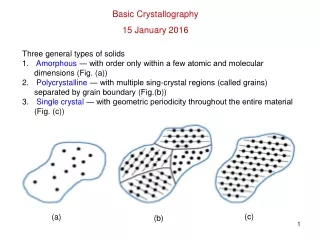
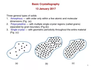
Basic Crystallography 24 January 2014 Three general types of solids • Amorphous ― with order only within a few atomic and molecular dimensions (Fig. (a)) • Polycrystalline ― with multiple sing-crystal regions (called grains) separated by grain boundary (Fig.(b)) • Single crystal ― with geometric periodicity throughout the entire material (Fig. (c)) (c) (a) (b) 1
Lattice: lattice: the periodic arrangement of atoms in the crystal Geometric Description of Single-Crystal — Space Lattices Unit cell: unit cell: a small volume that can be used to repeat and form the entire crystal. Unit cells are not necessary unique. 2
c b a Space lattices A general 3D unit cell is defined by three vectors Every equivalent lattice point in the 3D crystal can be found by c b a General case Special case 3
Basic Crystal Structures Three common types: Simple cubic Body-centered cubic (bcc) Face-centered cubic (fcc) and (c) (a) (b) 4
Why Crystal Planes Important? • real crystals are eventually terminate at a surface • Semiconductor devices are fabricated at or near a surface • many of a single crystal's structural and electronic properties are highly anisotropic
Find the intercept on the x, y, and z • Reduce to an integer. i.e. lowest common denominator • Take the reciprocal and reduce to the smallest set of integers (h, k, l) These are called the Miller Indices
(111) Plane with normal direction [111] (111) Plane with normal direction [111] (100) Plane with normal direction [100] (100) Plane with normal direction [100] (110) Plane with normal direction [110] (110) Plane with normal direction [110] Examples of Lattice Planes in Cubic Lattices
(001) (010) Set of Planes Due to the high degree of symmetry in simple cubic, bcc and fcc, the axis can be rotated or parallel shift in each of three dimensions, and a set of plane can be entirely equivalent. {100} set of planes: (100), (010), (001) Similarly, {110} set of planes: (110), (101), (011) 9
(001) (010) Set of Planes Due to the high degree of symmetry in simple cubic, bcc and fcc, the axis can be rotated or parallel shift in each of three dimensions, and a set of plane can be entirely equivalent. {100} set of planes: (100), (010), (001) Similarly, {110} set of planes: (110), (101), (011) 10
The Diamond Structure • Materials possess diamond structure: Si, Ge • 8 atoms per unit cell • Any atom within the diamond structure will have 4 nearest neighboring atoms 11
Volume Density of Atoms • Volume density Number of atoms per unit volume = Total number of atoms / volume occupied by these atoms = number of atoms per unit cell/volume of the unit cell Unit: m-3 or (cm)-3 • Example For Silicon a= 5.43 Å = 5.43 x 10⁻⁸ cm Volume density = 13
Raw material ― Polysilicon nuggets purified from sand Si crystal ingot Crystal pulling Slicing into Si wafers using a diamond saw A silicon wafer fabricated with microelectronic circuits Final wafer product after polishing, cleaning and inspection Procedure of Silicon Wafer Production 14
Identification of Wafer Surface Crystallization Flats can be used to denote doping and surface crystallization 15