Download
1 / 2
20 likes | 58 Views
Kensington is committed to providing the most reliable and innovative wafer handling robots, precision motion control stages, Foup Opener etc. If you are seeking to know more, talk to our team of experts.

E N D
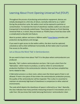
Learning Abo Learning About Front Opening Universal Pod (FOUP) ut Front Opening Universal Pod (FOUP) Throughout the process of producing semiconductor equipment, devices are initially developed on a thin disc of silicon, normally referred to as a ‘wafer’. During the production cycle, the wafers must not be exposed to particles or contamination. To maintain the level of cleanliness needed, wafers are only ever transported in hermetically sealed boxes. These boxes (known as Front Opening Universal Pods or, in short, they are known as ‘FOUPs) have a front face door with a complicated turnbuckle lock feature. Want to protect, deliver and store a 300mm wafer? Foup Opener provides safe protection during delivery and storage. If you want to gain access to the wafers within, the door must be captured, unlocked as well as then withdrawn horizontally, & then taken clear to provide free access to the wafers. Let us Discuss the Word ‘Fab’ in Semiconductors Let us Discuss the Word ‘Fab’ in Semiconductors Do you want to learn more about ‘Fab’? It is the place where semiconductors are produced. Basically, ‘Fab’ is where semiconductors are born. Fab is just a short form for ‘fabrication,’ which means to produce, as well as refers to semiconductor production facilities in the semiconductor industry. Here we have compiled key terms related to fabs. A fabrication process is a clean room, where even the tiniest speck of dust is not allowed. If even a tiny piece of dust enters the semiconductor production process, the quality of the semiconductor will be impacted. This is why it is essential to maintain an extremely high level of cleanliness in comparison to other external environments. The scale which depicts the cleanliness of space is referred to as ‘class’. Basically, the class indicates how many particles measuring at least 0.5 micrometers are in 1 cubic foot. Did you know that inside Samsung Electronics’ semiconductor clean
rooms have high-performance which can efficiently filter out the dust on the ceilings & through tiny lattice-shaped holes on the floor? A clean environment is well-maintained via a structure that circulates air from top to bottom. Before entering the area of the production environment, all workers are instructed to wear special cleanroom garments. The garments are designed especially for a clean room so that fine particles such as dust do not enter the lab and prevent static electricity. It may impact the semiconductor integrated circuit. FOUP (Front Opening Unified Pod/Front Opening Universal Pod) Undoubtedly, Semiconductors are produced after completing hundreds of steps which are represented by eight main processes. During these processes, the FOUP (Front Opening Unified Pod/Front Opening Universal Pod), as well as OHT (Overhead Hoist Transport), helps the wafers move efficiently to several facilities inside the fab. FOUP is basically a container that was designed to store or safely move wafers & it can be seen as a box which is dedicated to wafer delivery. OHT is a delivery vehicle that helps move this box to wherever it needs to go. The OHT is associated as the most standout piece of equipment in the fab. It helps quickly transport the FOUP, which consists of wafers, to the necessary equipment along railways which are installed like roads on the ceiling of the fab. Though it is exciting to enter and experience the semiconductor production area, this place may be even more interesting for those interested in semiconductors. I hope today’s post satisfies and involves your curiosity a bit. We hope you’ll look forward to the next 300mm FOUP discussion with us!