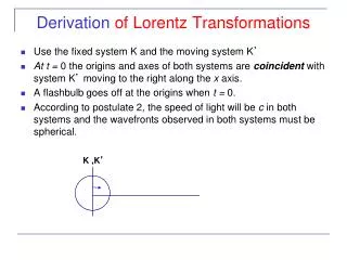
Qualitative Derivation
Chapter 6. pn Junction Diodes: I - V Characteristics. M ajority carriers. M ajority carriers. Qualitative Derivation. Chapter 6. pn Junction Diodes: I - V Characteristics. Current Flow in a pn Junction Diode.


Qualitative Derivation
E N D
Presentation Transcript
Chapter 6 pn Junction Diodes: I-V Characteristics Majority carriers Majority carriers Qualitative Derivation
Chapter 6 pn Junction Diodes: I-V Characteristics Current Flow in a pn Junction Diode • When a forward bias (VA > 0) is applied, the potential barrier to diffusion across the junction is reduced. • Minority carriers are “injected” into the quasi-neutral regions Δnp > 0, Δpn > 0. • Minority carriers diffuse in the quasi-neutral regions, recombining with majority carriers.
Chapter 6 pn Junction Diodes: I-V Characteristics Ideal Diode: Assumptions • Steady-state conditions. • Non-degenerately doped step junction. • One-dimensional diode. • Low-level injection conditions prevail in the quasi-neutral regions. • No processes other than drift, diffusion, and thermal R–G take place inside the diode.
Chapter 6 pn Junction Diodes: I-V Characteristics Current Flow in a pn Junction Diode • Current density J = JN(x) + JP(x) • JN(x) and JP(x) may vary with position, but J is constant throughout the diode.
Chapter 6 pn Junction Diodes: I-V Characteristics Carrier Concentrations at –xp, xn • Consider the equilibrium carrier concentrations at VA = 0: p-side n-side • If low-level injection conditions prevail in the quasi-neutral regions when VA 0, then:
Chapter 6 pn Junction Diodes: I-V Characteristics “Law of the Junction” • The voltage VA applied to a pn junction falls mostly across the depletion region (assuming that low-level injection conditions prevail in the quasi-neutral regions). • Two quasi-Fermi levels is drawn in the depletion region:
Chapter 6 pn Junction Diodes: I-V Characteristics Excess Carrier Concentrations at –xp, xn p-side n-side
Chapter 6 pn Junction Diodes: I-V Characteristics Example: Carrier Injection • A pn junction has NA=1018 cm–3 and ND=1016 cm–3. The applied voltage is 0.6 V. • a) What are the minority carrier concentrations at the depletion-region edges? • b) What are the excess minority carrier concentrations?
Chapter 6 pn Junction Diodes: I-V Characteristics Excess Carrier Distribution • From the minority carrier diffusion equation, • For simplicity, we develop a new coordinate system: • We have the following boundary conditions: • Then, the solution is given by: • LP : hole minority carrier diffusion length
Chapter 6 pn Junction Diodes: I-V Characteristics Excess Carrier Distribution • New boundary conditions • From the x’→ ∞, • From the x’ →0, • Therefore • Similarly,
Chapter 6 pn Junction Diodes: I-V Characteristics pn Diode I–V Characteristic n-side p-side
Chapter 6 pn Junction Diodes: I-V Characteristics pn Diode I–V Characteristic • Shockley Equation,for ideal diode • I0 can be viewed as the drift current due to minority carriers generated within the diffusion lengths of the depletion region
Chapter 6 pn Junction Diodes: I-V Characteristics Diode Saturation Current I0 • I0 can vary by orders of magnitude, depending on the semiconductor material, due to ni2 factor. • In an asymmetrically doped pn junction, the term associated with the more heavily doped side is negligible. • If the p side is much more heavily doped, • If the n side is much more heavily doped,
Chapter 6 pn Junction Diodes: I-V Characteristics Diode Carrier Currents • Total current density is constant inside the diode • Negligible thermal R-G throughout depletion region dJN/dx = dJP/dx = 0
Chapter 6 pn Junction Diodes: I-V Characteristics Excess minority carriers Excess minority carriers Carrier Concentration: Forward Bias • Law of the Junction • Low level injection conditions
Chapter 6 pn Junction Diodes: I-V Characteristics Carrier Concentration: Reverse Bias • Deficit of minority carriers near the depletion region. • Depletion region acts like a “sink”, draining carriers from the adjacent quasineutral regions
Chapter 6 pn Junction Diodes: I-V Characteristics No saturation “Slope over” “Breakdown” Smaller slope Deviations from the Ideal I-V Behavior • Si pn-junction Diode, 300 K. Forward-bias current Reverse-bias current
Chapter 6 pn Junction Diodes: I-V Characteristics Dominant breakdown mechanism is tunneling Empirical Observations of VBR • VBR decreases with increasing N, • VBR decreases with decreasing EG. • VBR : breakdown voltage
Chapter 6 pn Junction Diodes: I-V Characteristics Breakdown Voltage, VBR • If the reverse bias voltage (–VA) is so large that the peak electric field exceeds a critical value ECR, then the junction will “break down” and large reverse current will flow • At breakdown, VA=–VBR • Thus, the reverse bias at which breakdown occurs is
Chapter 6 pn Junction Diodes: I-V Characteristics Breakdown Mechanism: Avalanching High E-field: High energy, enabling impact ionization which causing avalanche, at doping level N < 1018 cm–3 Small E-field: • ECR : critical electric field in the depletion region Low energy, causing lattice vibration and localized heating
Chapter 6 pn Junction Diodes: I-V Characteristics Breakdown Mechanism: Zener Process • Zener process is the tunneling mechanism in a reverse-biased diode. • Energy barrier is higher than the kinetic energy of the particle • The particle energy remains constant during the tunneling process • Barrier must be thin dominant breakdown mechanism when both junction sides are heavily doped • Typically, Zener process dominates when VBR < 4.5V in Si at 300 K and N > 1018 cm–3.
Chapter 6 pn Junction Diodes: I-V Characteristics Effect of R–G in Depletion Region • R–G in the depletion region contributes an additional component of diode current IR–G. • The net generation rate is given by • ET: trap-state energy level
Chapter 6 pn Junction Diodes: I-V Characteristics Effect of R–G in Depletion Region • Continuing, • For reverse bias, with the carrier concentrations n and p being negligible, • Reverse biases with VA< – few kT/q
Chapter 6 pn Junction Diodes: I-V Characteristics Effect of R–G in Depletion Region • Continuing, • For forward bias, the carrier concentrations n and p cannot be neglected,
Chapter 6 pn Junction Diodes: I-V Characteristics Effect of R–G in Depletion Region Diffusion, ideal diode
Chapter 6 pn Junction Diodes: I-V Characteristics Effect of Series Resistance Voltage drop, significant for high I RS can be determined experimentally
Chapter 6 pn Junction Diodes: I-V Characteristics Effect of High-Level Injection • As VA increases and about to reach Vbi, the side of the junction which is more lightly doped will eventually reach high-level injection: (for a p+n junction) (for a pn+ junction) • This means that the minority carrier concentration approaches the majority doping concentration. • Then, the majority carrier concentration must increase to maintain the neutrality. • This majority-carrier diffusion current reduces the diode current from the ideal.
Chapter 6 pn Junction Diodes: I-V Characteristics High-Level Injection Effect Perturbation of both minority and majority carrier
Forward-bias current Chapter 6 pn Junction Diodes: I-V Characteristics Summary Deviations from ideal I-V Reverse-bias current Due to thermal generation in depletion region Due to high-level injection and series resistance in quasineutral regions Due to avalanching and Zener process Due to thermal recombination in depletion region
Chapter 5 pn Junction Electrostatics Homework • This time no homework. Prepare well for Quiz 2.