Download
1 / 11
110 likes | 130 Views
The PCB Assembly process has a number of steps- some of these are automated and some are manual. Even before we get to the Assembly process. Printed circuit board assembly process includes solder paste stenciling, reflow soldering, through-hole components, functional test and more.

E N D
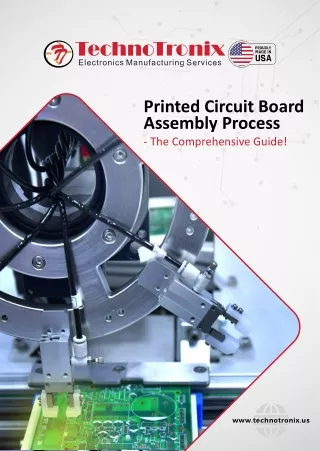
Printed Circuit Board Assembly Process - The Comprehensive Guide! www.technotronix.us
Table of Contents 01. About Printed Circuit Board 02. PCB Design 03. There are Basically 3 types of Printed Circuit Boards 04. How to choose between SMT & Thru-Hole 05. Preparatory Steps Prior to Assembly 06. Printed Circuit Board Assembly Process Flow: Solder Paste Stenciling Pick and Place Reflow Soldering Quality Control Through-Hole Components Func?onal Test 07. Through Hole Technology Assembly Process 08. SMT PCB Assembly Process 09. Mixed Technology 10. Contact Informa?on 02 www.technotronix.us 714/630-9200 sales@technotronix.us
About Printed Circuit Board The use of electronics has been growing exponen?ally in our lives. Not just that we are seeing miniaturiza?on as a rising trend when it comes to electronics. What makes all of this possible, however, are those small green chips that are at the heart of all electronic devices. Yes, we are referring to the Printed Circuit Boards or PCBs as they are popularly called. These are largely made of fiberglass; copper while being held together with epoxy and they are insulated with a solder mask. What gives these boards the complex func?onality that you witness in the electronic products, are the components and the way they are assembled. Essen?ally, a Printed Circuit Board with components mounted on it is known as an assembled PCB and this process of moun?ng components on the board is referred to as the PCB Assembly process. With the usage of PCBs becoming ubiquitous with increased usage of electronic products, it is important to understand the PCB Assembly process in detail. The PCB Assembly process has a number of steps- some of these are automated and some are manual. Even before we get to the Assembly process, let us look at aspects of PCB design, types of PCB available and the component moun?ng technologies used. 03 03 www.technotronix.us 714/630-9200 sales@technotronix.us
PCB Design • The base material of the PCB that gives the PCB its rigidity is known as the substrate • On each side of the PCB is a copper layer. • Above the copper layer is the solder mask. Essen?ally, what it does is to insulate the copper traces. The solder mask is therefore responsible for smooth working of the PCBA as it ensures that the soldering does not happen on unwanted parts. • The final layer on the PCB board is the silkscreen which adds labels and therefore indicates the func?on of the various components. 04 www.technotronix.us 714/630-9200 sales@technotronix.us
There are Basically 3 Types of Printed Circuit Boards. These Include: Rigid PCBs - As the name indicates, these are inflexible PCBs. For such PCBs the base is made of materials such as FR4, epoxy or phenolics. There are also metal core PCBs. As the name suggests they are made of a metal core that spreads heat efficiently and therefore components that are heat sensi?ve, are protected. Flexible PCB: Flexible PCBs offer more pliability than their rigid counterparts and therefore are of use in several applica?ons. Some of the other advantages offered by Flexible PCBs include: • They offer greater connec?vity • They are known for their reduced weight • They can absorb shocks and vibra?ons and are known for their durability • They are resistant to environmental forces such as heat, chemicals and more. Rigid-Flex PCBs: This is a hybrid design that essen?ally has the quali?es of both rigid and flexible PCBs. Typically, these are mul? layered with flexible circuit substrates joined with rigid boards. They find mul?ple applica?ons such as: • Applica?ons that are required to be highly reliable in the face of vibra?ons, shock etc. • High-density applica?ons • Applica?ons where there are 5 or more rigid boards. When it comes to the component moun?ng technology for printed circuit board assembly, two types of technologies find favour: Surface Mount Technology: Electronic products are marked by complex circuitry. A large number of electronics are today manufactured thus with Surface Mount Technology. This is par?cularly useful for small, sensi?ve components such as resistors or diodes. The main advantages of surface mount technology include: • It lends itself to automated produc?on and soldering • It is cost-effec?ve • It takes care of high component density • It offers be?er performance when the environment is subject to vibra?ons. It’s biggest disadvantage, however, is that when subject to high heat, it isn’t quite reliable. Thru-hole technology- This is useful when components are to be mounted on the board through a process of plugging them through holes on the board. When there are large components, this technology is preferable. The other advantages that accrue with Thru-hole technology include: • It creates strong bonds between the components and the board. In applica?ons like transformers, for example, where there is high heat, these work best • The components can be swapped out, so it lends itself to tes?ng and to prototypes. The disadvantages of thru-hole include the fact that the drilling is both expensive and ?me-consuming. It also restricts components on one side of the board. Overall, it is also more expensive. 05 www.technotronix.us 714/630-9200 sales@technotronix.us
How to Choose Between SMT & Thru-Hole When you are dealing with complex boards with small parts and high density, SMT is largely preferred. For large components, applica?ons that need to withstand heat, thru hole is the preferred choice. In many cases however, a combina?on of both may be the need of the hour. Preparatory Steps Prior to Assembly Prior to the PCB assembly process, however, there need to be some preparatory steps. This largely includes assuring that the design of the PCB is right for which a Design for Manufacturability test is undertaken. This is to ensure that no opera?onal issues are faced once the PCB is ready. A Design for Manufacturing check looks at the various design specifica?ons, any missing features and more, which can impact the func?onality of the PCB. For example, is the spacing between components too less, if so, if it not caught at the DFM stage, it could lead to short circuits at a later date. DFM can therefore go a long way in ensuring that costly errors are later avoided. Solder Paste Stenciling The first stage begins with the Solder Paste Stenciling. Essen?ally this means applying a solder paste on the board. A thin stencil is placed over the PCB, this allows the solder paste to be applied on certain parts of the PCB. Essen?ally, the solder paste is a mix of solder with the flux, which needs to be applied to the board at the correct places. Once the stencil is removed, the solder paste remains in the exact loca?on in which it was intended. 06 www.technotronix.us 714/630-9200 sales@technotronix.us
Printed Circuit Board Assembly Process Flow: Post the Design for Manufacturing (DFM) test comes the actual Circuit Board Assembly process. Pick and Place The next step is what is known as Pick and Place. A robo?c device now places the surface mount components on the printed circuit board. These are then soldered to the board. While earlier this process was manual, it is now automated that adds to precision and accuracy. Reflow Soldering This process ensures that the solder paste solidifies and that components are affixed to the board. Essen?ally, a?er pick and place the PCB board is moved to a conveyor belt. It is here that the board is heated to about 250 degrees Celsius, which melts the solder. Now it moves to cooler heaters where the solder cools and solidifies. This now connects the components to the printed circuit board. 07 www.technotronix.us 714/630-9200 sales@technotronix.us
Quality Control Rigid-Flex PCBs: This is a hybrid design that essen?ally has the quali?es of both rigid and flexible PCBs. Typically, these are mul? layered with flexible circuit substrates joined with rigid boards. They find mul?ple applica?ons such as: • Applica?ons that are required to be highly reliable in the face of vibra?ons, shock etc. • High-density applica?ons • Applica?ons where there are 5 or more rigid boards. Through-Hole Components The board also may contain a number of through-hole components, in which case these components require a special kind of soldering method. This could be manual soldering where components will be inserted one at a ?me. The process can be lengthy depending on how many components there are. There is also wave soldering which is an automated version. However, this isn’t possible for double-sided PCBs 08 www.technotronix.us 714/630-9200 sales@technotronix.us
Func?onal Test Post this comes the final inspec?on to test for func?onality. With simulated signals running through the PCB at this stage, its electrical characteris?cs are tested. This completes the PCB Assembly process. However, soldering can make the process messy. What is therefore extremely important, is to wash the product a?er the soldering process. For this, a high-pressure washing apparatus is used, where the PCB is washed in deionized water. Washing is then followed by a drying process which is then followed by packaging and shipment. It is also important to note that there are some differences between THT Assembly, SMT Assembly and Mixed Technology. Through Hole Technology Assembly Process In this Through Hole Assembly process the first step is that of component placement where components are placed manually conforming to a number of regula?ons regarding polarity and orienta?on of components. This is, then followed by a process of inspec?on. The last step is to do with wave soldering which involves the THT components to be accurately soldered onto the circuit board. 09 www.technotronix.us 714/630-9200 sales@technotronix.us
SMT PCB Assembly Process SMT Assembly process involves the steps of Solder Paste Prin?ng where the solder paste is applied through a solder paste printer. This is then followed by moun?ng of components through an auto pick-and-place machine that s?cks parts to the board. The final step is to do with reflow soldering which binds the components firmly to the board. Mixed Technology With electronic products becoming increasingly complex and miniaturiza?on becoming the order of the day, most boards have both thru-hole and SMD components. In such cases it is important to have a proper sequence in order. Hand soldering works well where there are many components on both sides and where SMD components are more. Where there are a small number of THT components, wave soldering is recommended. It is important to choose the right Printed Circuit Board Assembly (PCBA)USA who is technically sound and aware of all these nuances to do jus?ce to your project. At Technotronix, we have over 4 decades of experience in both PCB fabrica?on and assembly. Our big advantage comes from our state-of-the-art equipment but also our experienced team of engineers who is equipped with the industry best-prac?ces and ensures that you do not have to make any costly mistakes. In addi?on, our robust tes?ng procedures ensure that what you get are reliable products. You can count on us for prototypes as well as large runs. With encouraging turnaround ?mes, we are a go-to provider for clients across a wide variety of industries. In fact, a large body of clients who have complete faith in us, stands as the biggest tes?mony to our success. Technotronix offers professional PCB Assembly services with 4o years of exper?se. Our accurate PCB assembly process meets the quality standards, including ISO-9001:2015, RoHS, and more. You can rely on our PCB design tools that, in turn, lead to that perfect PCB Assembly. Our superior engineering capabili?es mean that each board matches your exact requirements and technical specifica?ons. In case if you have any ques?ons, please feel free to contact us via email at sales@technotronix.us Get a Quick Quote for PCB Assembly! 10 www.technotronix.us 714/630-9200 sales@technotronix.us
Contact Information 714/630-9200 714/630-9207 sales@technotronix.us 1381 N Hundley Street, Anaheim, CA 92806 www.technotronix.us