Download
1 / 8
80 likes | 201 Views
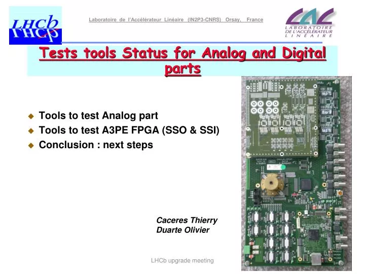
Tests tools Status for Analog and Digital parts. Tools to test Analog part Tools to test A3PE FPGA (SSO & SSI) Conclusion : next steps. Caceres Thierry Duarte Olivier. Tools to test Analog part. ADC emulation. SPY data. FIFO pattern Generate digital signals Check FPGA computations

E N D
Tests tools Status for Analog and Digital parts Tools to test Analog part Tools to test A3PE FPGA (SSO & SSI) Conclusion : next steps Caceres Thierry Duarte Olivier LHCb upgrade meeting
Tools to test Analog part ADC emulation SPY data • FIFO pattern • Generate digital signals • Check FPGA computations • SPY FIFO • storage of processing results • ANALOG PULSE FIFO • generate trigger of analog pulses 96 • PATTERN_FIFO 96 96 8 USB_data Buffer_FIFOs (12x8) USB wr WR RD (96 x 512) {Add 0x1C} 96 1 96 • Wr : USB • Rd : USB or 40 Mhz 96 96 8 1 (x8) 96 USB data 96 0 WR RD • 12 bit ADC data fromAnalog Mezzanine (96 x 512) 8 x 12bits {Add 0x06} setup_ register[9] • SPY_FIFO 0 USB_data • Wr : USB or 40 Mhz • Rd : USB setup_ register[8] 8 8 8 • ANALOG_PULSE_FIFO 8 • Analog Pulse • ( 1 per ADC Channels) ClkUSB WR RD 8 1 USB_data (8 x 512) {Add 0x1F} • Wr : USB • Rd : USB or 40 Mhz Clk 40 Mhz 0 A3PE setup_register[9] Trigger for Analog LHCb upgrade meeting
Tools to test A3PE FPGA (SSO & SSI) • Idea : RAM pattern to test the A3PE IOs functioning by exchanging data between the 2 FPGA (SSO and SSI) • USB Rd / Wr the RAM (To_AX and From_AX). Buffer_FIFOs 32 ClkUSB 1 32 • Sequence: • To_AX _RAM Rd/Wr by USB • Start commande • Loop on to AX_RAM until stop command • Programmable latency to capture data from To_AX_RAM to FROM_AX_RAM • To_AX_RAM CLK_1 Rd Wr 0 From Delay Chip (32 x 512) {Add 0x1D} • Wr : USB • Rd : USB or Clk_1 setup_register[11] 8 USB_data 32 32 32 32 32 32 32 • Ctrl. • Wr / Rd • pattern RegUSB 32 BUSMSB AXTOA3PE 32 _q _q1 setup_register[10] 32 • Start / Stop and latency (implemented !) 32 1 8 • From_AX_RAM 32 USB_data 32 32 Wr Rd 32 0 (32x 512) 32 32 {Add 0x1E} 32 setup_register[11] • Wr : USB or Clk_1 • Rd : USB BUSLSB AXTOA3PE 8 32 USB_data AX500 A3PE _q3 _q2 LHCb upgrade meeting
Buffer_FIFOs Start Stop Latency sequence 32 ClkUSB 1 32 • To_AX_RAM CLK_1 Rd Wr 0 From Delay Chip (32 x 512) {Add 0x1D} • Wr : USB • Rd : USB or Clk_1 setup_register[11] 8 USB_data 32 32 32 32 32 32 32 • Ctrl. • Wr / Rd • pattern RegUSB 32 BUSMSB AXTOA3PE 32 _q _q1 setup_register[10] 32 32 1 8 • From_AX_RAM 32 USB_data 32 32 Wr Rd 32 0 (32x 512) 32 32 {Add 0x1E} 32 setup_register[11] • Wr : USB or Clk_1 • Rd : USB BUSLSB AXTOA3PE 8 32 USB_data • Status: • Firmware implemented • Cycle ok • To debug : • Rd / Wr RAM • FPGA Download • Started tests of the third board AX500 A3PE _q3 _q2 START / STOP / LATENCY SEQUENCE STARTSEQ LATENCY Tunablelatency Loop Rd To AX RAM WrFrom AX RAM 512 wordswrited STOPSEQ LHCb upgrade meeting
Conclusion • Digital electronic is ok, several adjustment have been done . • Last adjustment of the tools to test A3PE FPGA (SSO & SSI). • Started tests of third mother digital board. • Should we considered a 8 channels prototype FEB for the beginning of 2013 with GBT (availability of the first GBT samples) ? • Common tests in Barcelona ? LHCb upgrade meeting
SPARE LHCb upgrade meeting
Reminder : Typical acquisition sequence Beginning L0 sequence WriteAcq Register (PC) 1 2 3 Time 1 3 2 Trigger Generator 1 2 3 Data readout by USB Write Data Ctrl 25 ns to 65,5µs Discret Time Beginning latency delay Recording data in RAM (512 points) FIFO full End of latency delay • PC write start sequence bit of Acquisition (Acq) Register. • Beginning of L0 sequence. • Each trigger pulse involve pulse shape. • At the end of the latency delay recording 512 points of data (Max). • At the end of the record the system write one “end of acquisition”bit in the Acq_Register. • The PC scrutinize the Acq_Register, when the “end of acquisition” is high the PC download data with the USB interface. LHCb upgrade meeting
Clock tree LHCb upgrade meeting