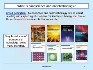
What is nanoscience and nanotechnology?
What is nanoscience and nanotechnology?. Broad definition - Nanoscience and nanotechnology are all about relating and exploiting phenomena for materials having one, two or three dimensions reduced to the nanoscale. . Very broad area of science and technology having many branches.

What is nanoscience and nanotechnology?
E N D
Presentation Transcript
What is nanoscience and nanotechnology? Broad definition - Nanoscience and nanotechnology are all about relating and exploiting phenomena for materials having one, two or three dimensions reduced to the nanoscale. Very broad area of science and technology having many branches. Introduction
Nanophysics: Main trends and crossroads Nano-Optoelectronics Nanophotonics Nanoelectronics Nano-Optomechanics Nano-Electromechanics Nanomechanics Introduction
Nanoscience is referred to as a research area devoted to studies of various phenomena in small-size devices. It is a cross-disciplinary field including physics, chemistry, and to some extent biology. The heart of nanoscience is mesoscopic physics. The word ``meso'' reflects the fact that the size of the systems under consideration is located between microscopic (atoms) and macroscopic scales. Introduction
Length scale Atoms Molecules & Clusters Electron mean free path Bulk materials Micro Macro Characteristic scales in nanoscience Nanometer scale Meso Modern electronic devices belong to mesoscopic scale Introduction
CMOS TECHNOLOGY • Intel’s Prescott processor • (released March 2004): • 150 million transistors • 90 nm design rules • 3.4 GHz clock frequency • DRAM chips: • 4 Gb chips demonstrated • (~ 109 transistors/cm2) Now chips based on the design rules of 22 nm are on the way. Intel’s Norwood (Pentium 4 - 130 nm) processor In 2004 we were already inside nanotechnology! Introduction
Main ingredients of nanoelectronics • Two-dimensional electron gas (2DEG) • Quantum wires and point contacts • Quantum dots • Nano-electro-mechanical systems • Carbon and non-carbon nanotubes and other molecular devices • Devices using superconductivity and magnetism at nanoscale • Devices for quantum computation • Spintronics – manipulation electron spin Novel devices Introduction
Examples Introduction
2DEG is a generic object for new physics Nobel Prizes 1985, 1998, 2000 It serves as a building block for electronic devices Metal-Oxide-Semiconductor (MOS) structures 2DEG is formed at the semiconductor-insulator interface Semiconductorheterostructure 2DEG is formed at the interface between two semiconductors Band gap engineering Two-dimensional Electron Gas (2DEG) Introduction
Cleaved structures Point contacts Quantum Wires and Point Contacts Split-gate structures “Back-end” parts of nanodevices Carbon nanotubes Introduction
Lateral quantum dots Coulomb blockage! Artificial atoms – new periodic table Vertical Quantum Dots Ivar Giæver Introduction
Gate Repulsion at the dot Electron Dot Cost Attraction to the gate At the energy cost vanishes ! Coulomb blockade Single-electron transistor (SET) Introduction
Self-assembled quantum dots are periodic arrays of “artificial atoms”. They are considered to be promising systems for heterostructure lasers. Our project: Ge-in-Si arrays Introduction
SINGLE-ELECTRON SINGLE-MOLECULE TRANSISTORS see also: - E. S. Soldatov et al. (1996) - H. Park et al. (2000) - N. Zhitenev et al. (2002) - S. Kubatkin et al. (2003) J. Park et al. (2002) Molecular electronics SET within the “Orthodox” theory: Introduction
Growth Fabrication Characterization MBE STM EBL Quantum corrals Instrumentation for nanoscience and nanotechnology Introduction
Even a modest nanocenter needs: • Start-up for instrumentation for > 20 mil. US $ (in addition to a proper building) • Proper running costs (rather high) • Research personnel highly qualifiedboth in experiment and theory The center will not be efficient without all these ingredients. Introduction
QM: Particle or wave? Quantum modes in the wire 1 2 2 New laws of Nature at nanoscale? In a classical resistor, the resistance is due to electron scattering. Otherwise electrons are just accelerated by the electric field. Introduction
Classical versus quantum physics Introduction
Quantization of conductance vs. gate voltage! New universal unit of resistance –h/e2 Absent in classical theory Introduction
Basic problems • Nanoscale systems require understanding • Quantum transport • Role of electron-electron interaction, which is more pronounced in low-dimensional systems • Role of disorder • Role of contacts and electromagnetic environment • Nano-devices are usually out of equilibrium, which requires special understanding All these issues are far from being fully understood New research area with rich physics and chemistry! Introduction
Quantum Mechanics of Interacting Particles Condensation Wigner crystal Introduction
Nanomaterials Encapsulated 4 nm Au particles self-assembled into a 2D array supported by a thin film, Anders et al., 1995 Scheme for molecular manufacturing Nano-electromechanical systems Introduction
Concrete systems Electron “shuttles” Molecular motors Carbon nanotubes In nanomaterials electrical and mechanical energies are comparable Electrical and mechanical modes are strongly coupled Nano-electro-mechanics Introduction
“Shuttle” transfer of electrons A movable cluster “conveys” electron one by one In some cases electro-mechanic instabilities can take place “Shuttle” transport has been observed in several concrete systems Introduction
Solar cells with nanoparticles: Nanoplasmonics Main principle: Plasmon resonances due to nanoparticles strongly enhance the time, which photons spend close to the active layer Metallic nanoparticles embedded in the host system close to the active layer Key players: Centre for Sustainable Energy Systems at the Australian National University (ANU) ; Caltech, US; FOM-Institute, AMOLF, the Netherlands. Simulation of increased light intensity beneath a metal nanoparticle on a silicon cell Introduction
x J B(r) l B dA = 0 Fluks kvantum: 2003 Mesoscopic Superconductivity Studies of individual magnetic vortices by magneto-optical (MO) imaging Tom Henning Johansen et al., Univ. Oslo Introduction
prøvekant One can take snapshots at different times, and in this way observe vortex dynamics Example: Edge effects MOI single vortices allows to study and influence mesoscopic structure of vortex matter Introduction
Classical length – electron mean free path, More about physical scales Quantum length – de Broglie wavelength of an electron having the Fermi energy: This scale is relevant to the size quantization – quantum films, wires, and dots Introduction
Another important scale – phase coherence length, Scale introduced by Coulomb interaction and depending on the device capacitance, C - relevant tosingle-electron tunneling Interplay between different scales leads to a rich picture of transport through nanosystems. The specific properties of different regimes can be used for various applications. Introduction
Basic classification of transport regimes Introduction
Ballistic transport, , quantum point contact To the left, the surface topography of a GaAs microchip is shown. The picture has been taken with an atomic force microscope. The chip hosts a quantum film about 30 nm below its surface, which is removed underneath the bright lines. A small and short wire of length 140 nm and width 80 nm connects source and drain. The measurement to the right shows the conductance of the wire as a function of the gate voltage. At low temperatures, a conductance quantization in units of 2e2/h is visible, which vanishes around 20 K. Introduction
Classical The quantum Hall effects and Shubnikov-de Haas oscillations Hall effect Shubnikov-de Haas oscillations and the quantum Hall effect. We look at a measurement of the longitudinal and the Hall resistance (Rxx and Ryy, respectively), of a two dimensional electron gas, as a function of a magnetic field applied perpendicular to the plane of the quantum film. The experiment has been performed at a temperature of 100 mK. The Hall resistance is quantized in units of h/2e2. Introduction
At low temperatures The resistance of a small ring with a diameter of about 1 micron (the light gray areas in the inset) as a function of a magnetic field applied perpendicular to the ring plane shows periodic oscillations, known asAharonov-Bohm oscillations. They indicate that a significant fraction of the electrons traverse the ring phase coherently. Phase coherence Introduction
Single-electron tunneling and quantum dots The right inset shows again the surface topography of a semi- conductor with a two dimensional electron gas underneath. The bright lines enclose a small island. It is coupled to source and drain via two quantum point contacts, forming tunnel barriers for the electrons. The barriers are tuned by adjusting the voltages at the gates Ql and Q2. The main figure shows the conductance through the island as a function of the gate voltage VI applied to region I. VItunes the potential of the island. The conductance peaks indicate that only for a particular island potential, electrons can be transferred between the island and the leads. The left inset shows a fit to a function one would expect for peaks that are governed by thermal smearing of the Fermi function. Introduction
New systems:Carbon nanotubes, etc Structure of a carbon nanotube. The circles denote carbon atoms in a graphite sheet, which is rolled up and forms a tube with a diameter of a few nanometers. The ends are supposedly capped by a carbon hemisphere. Samples, materials, and experimental techniques Semiconductor devices:GaAlAs heterostructures (optoelectronics, high mobility under modulation doping) Si-MOSFET (silicon has a natural oxide, that is very important) Introduction