Download
1 / 20
230 likes | 821 Views
Time-Resolved Thermoreflectance Imaging for Thermal Testing and Analysis . Dr. Mo Shakouri Chairman Microsanj , LLC., Silicon Valley USA. info@ microsanj.com. Applications. Outline. Motivation Instrumentation Lock-in mechanism Imaging through silicon (near IR) Diffusion length

E N D
Time-Resolved Thermoreflectance Imaging for Thermal Testing and Analysis Dr. Mo Shakouri Chairman Microsanj, LLC., Silicon Valley USA info@microsanj.com
Applications SEMICON JAPAN 2013 - MICROSANJ
Outline SEMICON JAPAN 2013 - MICROSANJ • Motivation • Instrumentation • Lock-in mechanism • Imaging through silicon (near IR) • Diffusion length • Examples Small hotspot / Logic circuitry / Emission / Depth in metal layers • Summary
Challenges on thermal characterization SEMICON JAPAN 2013 - MICROSANJ General challenges for electronics devices Small features: 10s nm – 100s microns – difficult to contact High speed response due to the small thermal mass Highly non-uniform Additional challenges for photonics and power devices Light emission (photonics) High heat density Heat sinks requirement (power devices)
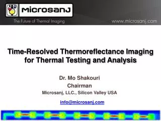
Thermoreflectance imaging setup Console box Microscope setup CCD Sig. gen. Temp. contl. LED Control box. Objective lens DUT SEMICON JAPAN 2013 - MICROSANJ
How it works - thermoreflectance LED driver GP-IB Power LED PC Light Detector CCD, InGaAs Microscope Objective Pulse generator & power amp Device Thermal bed Thermoreflectance coefficient System diagram SEMICON JAPAN 2013 - MICROSANJ
Lock-in signals Timing chart 4ms @ 25% Duty Cycle t0 Device Excitation 1ms CCD exposure 33ms @ 30Hz delay 100ms t0 t1 t1 LED pulse Temperature Acquisition timing (shifting by cycle) Temperature data point along the bias cycle SEMICON JAPAN 2013 - MICROSANJ
Through silicon and emission Top view InGaAs CCD 1300 nm LED Objective Substrate Transmittance vs Wavelength, Si Bottom view (Image from http://www.janis.com) Flip Chip DUT resolution % Transmittance 1.0 10.0 Wavelength, mm SEMICON JAPAN 2013 - MICROSANJ
Defects and signature of potential failure Emission – sign of high density of electron collisions Thermal hotspot – location of potential long-term reliability Thermal foot print irregular local energy spot Arrhenius's law Transient irregular timing - potential of logic/operation failure Near Infrared (NIR) wavelength provide a capability of both thermal signal and emission simultaneously. LED options: 1050, 1200, 1300, and 1500 nm SEMICON JAPAN 2013 - MICROSANJ
Resolution and sensitivity Temperature n : number of averaging due to the weak signal (Cth ~ 10-4 order) • Spatial resolution Visible wavelengths, d ≈ 250-300 nm NIR d ≈ 500 nm d ≈ l/2 • Time resolution As scaling smaller, time resolution must be smaller due to thermal diffusion. Dt : 100ns for our setup. (for 1% error in temperature) • Emission InGaAs uncooled camera effective sensitivity of one pixel for emission ~ 30 mW/mm2 SEMICON JAPAN 2013 - MICROSANJ
Examples - Small hotspot 60 50 40 40 a) 1.4mmgate on MOSFET 1.4 mm gate on MOSFET Temperature (a.u.) 30 20 10 0 b) 12 10 0 8 6 4 2 Distance (mm) SEMICON JAPAN 2013 - MICROSANJ
Transient Behavior of IC Latch-Up Movie1 - Potential timing failure - 0.5 ms 0.7 ms 0.9 ms 1.0 ms 3.0 ms The latch-up location is circled in yellow SEMICON JAPAN 2013 - MICROSANJ
Thermal and emission overlay images Through silicon substrate, 450 mm thick. 5x Thermal signals LED l = 1300nm and InGaAs camera (640 x 512) 50x Emission signals 44 mW SEMICON JAPAN 2013 - MICROSANJ
Diffusion time/depth estimations m: depth of heat source a: thermal diffusivity [m2/s] t: time to reach observing surface SEMICON JAPAN 2013 - MICROSANJ
Examples - Through silicon, deep under the 6th metal layer Movie2 2.0 msec 0.97V, ~12mA, ~12mW 20% duty cycle 10 minutes of averaging (repeating) SEMICON JAPAN 2013 - MICROSANJ
Time delay to reach to the surface Precise time resolution is a key to find the response. SEMICON JAPAN 2013 - MICROSANJ
Microsanj, a technology leader inthermal imaging field • Major Customers • Chip Test Solutions • Design Engineering Inc. (DEI) • Infinera • Instituto de Microelectronica de Barcelona (CSIC) • Intel Corporation • NanyangTechnological University • Purdue University • Raytheon • Silicon Image • University of California Santa Barbara • Collaborative Research Activities • A*Star Singapore • Altera Corporation • Birck Nanotechnology Center at Purdue University • Nvidia • Philips Electronics • Qualcomm • Silicon Frontline • Si-Ware Systems • ST Microelectronics • Texas Instruments (National Semiconductor) • University of California at Santa Cruz SEMICON JAPAN 2013 - MICROSANJ • Founded by a team of PhDs from CalTech, Stanford, and UCSC in 2007 • More than 30 papers published to date
Summary High speed time-resolved thermoreflectance imaging is introduced. NIR illumination provides a through Si and electron emission Lock-in thermography and EMMI are compared. Examples demonstrated: Hotspots ~ 1mm, emission and thermal overlay, and a hotspot underneath 6 metal layers SEMICON JAPAN 2013 - MICROSANJ
Microsanj社の 開発した熱画像解析装置、Nanothermシリーズは、これまでのIRによるサーモグラフィー装置とは 全く異なった温度測定技術を用いたシステムです。測定物のIR放射を測定するのではなく、 測定物に非常に短時間の光を照射し、その反射光を計測することにより温度分布を測定するため、 測定物に全く影響を与えること無く、IRでは難しかった広い温度範囲を非接触にて測定することが 可能となりました。測定は金属を含むあらゆるものが可能で、測定物を熱したり、表面に特別な処理を 行う必要が有りません。また、薄いシリコン基板は光を透過することから、flip-chip等の、シリコン基板上の 半導体の熱画像を裏面から観測することが可能です。また、Nanothermシステムの最大の特徴として、 オプションにてバイアス電源と信号源を追加することにより、熱画像の過渡特性を、最速では0.8nsec間隔で 測定することができます。Nanothermシステムにより、温度上昇、熱集中の状況をリアルタイムに観察することで、 半導体そのものや半導体回路の最適な熱設計を行うこと、また故障解析、不良解析を行うことが可能です。 測定物の大きさは最小300nm、温度分解能は最小0.2℃、測定温度範囲-265~500℃に対応します。 ATN Japan 1-35-16 Nakagawa-Chuo Tsuzuki, Yokohama, Kanagawa, 224-0003 JAPAN Website: www.atnjapan.com E-mail: sales@atnjapan.com SEMICON JAPAN 2013 - MICROSANJ
Transient thermal/emission imaging SEMICON JAPAN 2013 - MICROSANJ