Download
1 / 48
480 likes | 510 Views
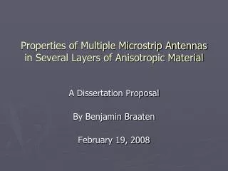
This Ph.D. thesis by Benjamin D. Braaten explores the properties, applications, and research on printed antennas embedded in stratified uniaxial anisotropic dielectrics, focusing on derivation and solving of spectral domain immittance functions, numerical results, and future work. The introduction covers the history and uses of microstrip antennas, advantages, disadvantages, and properties of interest like input impedance and radiation patterns. The proposed research aims to determine input impedance and mutual impedance in layered anisotropic structures, with relevance to microstrip antenna arrays, frequency-selective structures, RFID, and more. The study involves defining Hertz vector potentials, magnetic and electric fields, and Fourier transforms for analysis.

E N D
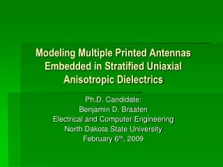
Modeling Multiple Printed Antennas Embedded in Stratified Uniaxial Anisotropic Dielectrics Ph.D. Candidate: Benjamin D. Braaten Electrical and Computer Engineering North Dakota State University February 6th, 2009
Topics • Introduction • The printed antenna. • Properties and applications. • Proposed research • Derivation of the new spectral domain immittance functions. • Solving the new spectral domain immittance functions. • Numerical results and measurements. • Future work. • Conclusion. North Dakota State University
Introduction • In 1953 Deschamps formally introduced the microstrip antenna [1]. • Many uses: • Radar • Cellular comm. • Satellite comm. • Wireless networks • Wireless sensors • Biomedical devices • RFID … [1] G. A. Deschamps, “Microstrip Microwave Antennas,” 3rdUSAF Symposium on Antennas, 1953. North Dakota State University
Introduction • Disadvantages: • Many designs have a narrow bandwidth • Radiate into a half space • Poor endfire radiation • Poor isolation between the feed an radiating elements • Possible surface waves (power loss) • Advantages: • Low profile • Lightweight • Low cost • Able to achieve UWB (in some cases) • Dual frequency capabilities • Simple to fabricate North Dakota State University
Introduction • Region between plates act like the region between a transmission line and a ground plane with both ends open. • Results in a standing wave. • Fringing fields are responsible for radiation. North Dakota State University
Introduction • Properties of interest include: • Input impedance • Current distribution • Radiation patterns • Bandwidth • Feed techniques • Mutual coupling with other elements • Conducting patch layout • … etc. North Dakota State University
Introduction Many different types of layouts exist: [2] [3] [2] Anthony Lai and Tatsou Itoh, “Composite Right/Left Handed Transmission Line Metamaterials,” IEEE Magazine, September 2004. [3] H. Wang, X. B. Huang and D. G. Fang, “A single layer wideband U-slot microstrip patch antenna array,” IEEE Antennas and Wireless Propagation Letters, vol. 7, 2008, pp. 9-12. North Dakota State University
Proposed Research Consider: North Dakota State University
Proposed Research RESEARCH QUESTIONS: What is the input impedance of a driven element in the layered anisotropic structure in the presence of other conducting patches defined on arbitrary anisotropic layers in the same structure? and • What is the mutual impedance between a driven element in the layered anisotropic structure and other conducting patches defined on arbitrary anisotropic layers in the same structure? North Dakota State University
Proposed Research The previous two questions are very significant in many fields. • Microstrip antenna arrays [4]. • Frequency Selective Structures (FSS) [5] • Radio Frequency Identification (RFID) [6] • IC based antennas • Radar … [4] David M. Pozar and Daniel H. Schaubert, “Microstrip Antennas: The analysis and Design of Microstrip Antennas and Arrays”, IEEE Press, Piscataway, NJ, 1995. [5]A.L.P.S. Campos an A.G. d'Assuncao, “Scattering paramters of a frequnecy selective surface between anisotropic dielectric layers for incidnet co-polarized plane waves,” IEEE Antennas and Propagation Society International Symposium, 2001, Vol. 4, July 8-13, 2001, p. 382-385. [6]K. Finkenzeller, RFID Handbook:Fundamentals and Applications in Contactless Smart Cards and Identification, John Wiley and Sons, West Sussex, England, 2003. North Dakota State University
The new spectral domain immittance functions Start with the following Hertz vector potentials: Electric Hertz potential and Magnetic Hertz potential North Dakota State University
The new spectral domain immittance functions • Next, only the y-direction of the Hertz vector potential is needed. and • This is because the optical axis is in the y-direction and • this component satisfies the higher order TE and TM tangential boundary conditions. North Dakota State University
Numerical results and measurements The TEM, TM and TE modes TEM mode TM and TE modes [9] [9] http://www.ibiblio.org/kuphaldt/electricCircuits/AC/02407.png North Dakota State University
The new spectral domain immittance functions Now define the following expression for the magnetic and electric field: where the Hertzian vector potentials are solutions to the following wave equations: North Dakota State University
The new spectral domain immittance functions and North Dakota State University
The new spectral domain immittance functions To simplify evaluating the previous expressions, we define the following Fourier transform: This results in the following relations: North Dakota State University
The new spectral domain immittance functions This results in the following simplified expressions: where and North Dakota State University
The new spectral domain immittance functions Similarly for and North Dakota State University
The new spectral domain immittance functions Single layer problem North Dakota State University
The new spectral domain immittance functions Single layer problem Now use these expressions to enforce the boundary conditions: North Dakota State University
The new spectral domain immittance functions Single layer problem After extensive factoring and manipulation, the following spectral domain immittance functions are derived: and (typical expression – spectral domain Green’s function) where North Dakota State University
The new spectral domain immittance functions Double (d3 = 0) and Triple layer problems North Dakota State University
The new spectral domain immittance functions Double and Triple layer problems After extensive factoring and manipulation, the following spectral domain immittance functions are derived: and North Dakota State University
Solving the new expressions • The spectral domain moment method was used to solve for the unknown current. • PWS functions were used as expansion and basis functions. • A delta source was used to drive the problem. North Dakota State University
Numerical results and measurements The problem chosen to validate newly derived spectral domain immittance functions was the printed dipole. North Dakota State University
Numerical results and measurements The first step was to validate the numerical results with experimental measurements. • Radius a = 0.4 mm • Length L = 60 mm • FR-4: εr = 4.35 • Printed strip W = 4a North Dakota State University
Numerical results and measurements Picture of measured monopole. North Dakota State University
This resulted in the following measured resonant frequencies:(Epsilam-10: and , Rogers 5880: ) Numerical results and measurements North Dakota State University
Numerical results and measurements Single layer results North Dakota State University
Numerical results and measurements Single layer results L = 15 mm W = 0.5 mm d1 = 1.58 mm Notice the y- component has the most effect on the resonant frequency (TM0 mode). North Dakota State University
Numerical results and measurements Single layer results The TEM, TM and TE mode reminder A quick illustration of the TM0 mode. TM and TE modes [9] [9] http://www.ibiblio.org/kuphaldt/electricCircuits/AC/02407.png North Dakota State University
Numerical results and measurements Single layer results North Dakota State University
Numerical results and measurements Single layer results North Dakota State University
Numerical results and measurements Single layer results L = 15 mm W = 0.5 mm f = 500 MHz d1 = 1.58 mm Notice:TM0 has the most effect (i.e. y-compontent of the permittivity North Dakota State University
Numerical results and measurements Double layer results North Dakota State University
Numerical results and measurements Double layer results L = 15 mm W = 0.5 mm d1 = 1.58 mm d2 = 1.58 mm ε1= 2.55 Notice: εx2affects the resonant frequency the most. North Dakota State University
Numerical results and measurements Double layer results The field lines: North Dakota State University
Numerical results and measurements Double layer results L = 15 mm W =0 .5 mm d1 = 1.58 mm ε1= 2.55 region 2: anisotropic North Dakota State University
Numerical results and measurements Double layer results L = 15 mm W = 0.5 mm f = 500 MHz d1 = 1.58 mm d2 = 1.58 mm ε1= 3.25. North Dakota State University
Numerical results and measurements Double layer results (Single layer results) North Dakota State University
Numerical results and measurements Double layer results L = 15 mm W = 0.5 mm f = 500 MHz d1 = 1.58 mm d2 = 1.58 mm ε1= 3.25. North Dakota State University
Numerical results and measurements Double layer results North Dakota State University
Numerical results and measurements Triple layer results L = 15 mm W = 0.5 mm f = 500 MHz d1 = 1.58 mm d2 = 1.58 mm d3 = 1.58 mm ε1= ε2= 3.25. North Dakota State University
Numerical results and measurements Triple layer results (Double layer results) North Dakota State University
Conclusion • New spectral domain immittance functions have been derived. • The new spectral domain immittance functions have been validated with measurements, published literature and commercial software. • One, two and three layer problems have been investigated. North Dakota State University
Conclusion • The following has been shown: • The permittivity in the direction of the optical axis below the printed dipole has the most impact on the resonant frequency. • The layer thickness values eventually have little effect on the resonant frequency. • The permittivity in the direction of the optical axis above printed dipoles has little or no effect on the mutual coupling. • The permittivity in the direction orthogonal to the optical axis in the layers above the dipoles can be used to control the mutual coupling. North Dakota State University
Conclusion • Future work • Investigate coupling between rectangular microstrip antennas in layered anisotropic diel. • Investigate coupling between UWB antennas in layered anisotropic diel. • Investigate how anisotropic materials could be used to control coupling between RFID tags • IC based antennas • Metamaterial based designs • Mathematical aspects • poles • surface wave modes • convergence North Dakota State University
Questions Thank you for listening North Dakota State University