Download
1 / 25
250 likes | 385 Views
Caltech collaboration for DNA-organized Nanoelectronics. The Caltech DNA-nanoelectronics team. State of the art, DNA self-assembly 1, DNA origami. State of the art DNA self-assembly 2, DNA tiles, tubes and crystals. State of the art DNA self-assembly 3, algorithmic + combination. Pd.

E N D
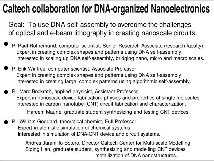
Caltech collaboration for DNA-organized Nanoelectronics The Caltech DNA-nanoelectronics team
State of the art DNA self-assembly 2, DNA tiles, tubes and crystals
State of the art DNA self-assembly 3, algorithmic + combination
Pd Si/ SiO2 Challenges for DNA organized nanoelectronics 1A + +
Challenges for DNA organized nanoelectronics 1B 50 nm To make nanostructures more rigid and to avoid aggregation origami-ribbon hybrids are used. red and blue hooks red tube blue tubes MOSFETgeometry crossbar Gate Channel
Challenges for DNA organized nanoelectronics 1C -- - --Vg= 0.5V -- --Vg= -0.5V ------ Vg= 0.5V 200 400 ISD [nA] 100 300 0 ISD[nA] -0.5 0.0 0.5 200 VSD [V] 100 V = 0.85V SD 0 -0.5 0.0 0.5 1.0 Vg [V] Over 30% of tubes are within 10 degrees of the desired orientation Orientation of SWNT 40 2% 22% 35 Red side (-1) Unknown (0) Blue side (1) 30 25 76% Frequency 20 15 10 5 0 0-20 20-40 40-60 60-80 80-100 100-120 120-140 140-160 160-180 Angle Characterization of DNA self-assembled CNT FET b a VSD ISD Vg ISD
Bockrath’s Aims Bockrath's Aims : To use short length-sorted carbon nanotubes to increase the yield of existing devices. (Many problems arise from very long tubes acting as bridges between multiple origami). To self-assemble and characterize circuits of more than one carbon-nanotube based device to create elementary logic gates and memory elements. To self-assemble novel devices to explore transport physics in nanostructures.
Vs Vout Vin Vs Vout Vs Vs Vout Vin2 Vin1 Rationally Engineered Logic gates and Memory Elements Utilizing Multiple Nanotubes Nanotube assembly Schematic circuit diagram Inverter SRAM NOR
V Novel Devices Probing Transport Physics in Nanostructures: Phase Coherence in Strongly-Interacting Electron Systems Novel Devices Probing Transport physics Many possibilities exist for making novel devices. DNA origami template for parallel nanotubes Tunable separation with desired values ~5-20 nm B Interferometer device source drain I Nanotubes act as a “which path?” interferometer enabling the study of phase coherent transport in Nanotube-based Luttinger liquids via a transport experiment. The setup is analogous to a double slit experiment in optics. The magnetic field B tunes the phase by the Ahoronov-Bohm effect. Tubes must be closer together than the phase coherence length in the electrodes, which is readily obtainable using DNA based self-assembly.
LUMO HOMO DNA-origami CNT-based Transistor Junctions V Theory and Modeling to Describe… DNA I CNT CNT Organic molecule • Size of molecules << scattering lengths (e.g. mean free path, de Broglie wavelength, etc.) -> quantum descriptions necessary. • Quantum chemistry of molecule(s)+nanotube -> charge flow & bonding -> geometry & energy spectrum of the entire system. • Organo-metallic interface mechanics and transport. Need to treat molecule as finite and nanotubes as semi-infinite electrodes. • Escape currents (through organic insulator layer). • Conformation effects on electronic transport. • Effect of finite bias. • IV characteristic of self-assembled CNT-based transistor junctions.
m 1 2 G1 G2 T(E,V) Molecular Mechanics Dynamics Multiscale Methodology:1st-principles I-V validated by rotaxane modeling geometry Density-functional theory (Hohenberg-Kohn-Sham) electro-chemical potential Green’s ftn. Formalism (Fisher-Lee) self-energy contact widening transmission Ballistic transport theory (Landauer, Buttiker) current e.g. Rotaxane switch dI/dV conductance
T(E) I(V) Au (111) Further validation: bi-phenyl-dithiol modeling contact molecule contact
Budget for 4 years, $2.6 million including: PI: Paul Rothemund: $200K/yr for Senior Research Associate salary and materials Budget Co-PI: Mark Bockrath $100K/yr for 1 graduate student and materials Co-PI: Bill Goddard $100K/yr for 1 graduate student and materials Co-PI: Erik Winfree $100K/yr for 1 graduate student and materials Equipment $150K/yr including plasma etcher/cleaner ($20K), wafer-scale Atomic Force Microscope ($200K) temperature-controlled dynamic light scattering ($50K).