Download
1 / 1
20 likes | 236 Views
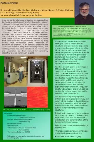
Nanoelectronics Dr. James E. Morris, Hui She, Tony Muilenburg, Vikram Kopuri, & Visiting-Professor C.S. Cho (Sangju National University, Korea) www.ece.pdx.edu/Labs/nano_packaging_lab.html. E-Beam. AFM. SET. Source. Drain. Gate. Cr nanodots.

E N D
Nanoelectronics Dr. James E. Morris, Hui She, Tony Muilenburg, Vikram Kopuri, & Visiting-Professor C.S. Cho (Sangju National University, Korea)www.ece.pdx.edu/Labs/nano_packaging_lab.html E-Beam AFM SET Source Drain Gate Cr nanodots Since conventional electronic devices are approaching the fundamental physical limit of miniaturization, interest in devices that can ensure further progress in electronics has quickened in the past decade. A possible path in this area is the fabrication of devices where the transfer of a single electron or a few electrons can be controlled. One such device is the single electron transistor (SET), in which the electrons are transferred one at a time by tunneling to and from nanometer-scale metal particles. One feasible method to make these nano-particles is to pattern the devices by using atomic force microscope (AFM) deposition of chromium, for example, asan adhesion promoter and seed on an insulator, fixing the nanodot positions, and stabilizing them. The nano-particles of the correct size and separation are thenformed by selectively depositing a noble metal, such as gold. The energy consumption and the size of electronic devices can be reduced dramatically by such technologies as the single-electron transistor (SET), and with significant improvement in operating speeds. Large-scale SET DRAM chips have been demonstrated by Hitachi. • In one project, a chromium-coated AFM tip is used to define the SET structures and positions by depositing a few chromium seed atoms on a flat silicon dioxide surface.An electron beam evaporation system is utilized to deposit gold metal and grow nano-particles on the chromium seeds by surface diffusion. The fabrication technique improves both reproducibility and reliability. • Another project goal is to investigate SET reliability issues and sensor applications. These reliability studies build on earlier work on discontinuous island metal films. A new successful conduction model for these films has application to SETs, and is being developed further to model more practical structures, with parallel experiments for validation. Regularly structured nanodot arrays will also be studied for optical properties and for threshold switching effects. • The optical absorption properties (which give gold-glass its rich ruby-red color) will be studied in the Optiprobe, recently donated by Intel. This work will be accompanied by extension of current theory to more practical structures. • Robust switching structures have been fabricated by plasma polymerization. Work here is focused on threshold stabilization and determination of the fundamental mechanism. • Related new projects being started in this field are: • Nanopackaging (nanotechnologies in electronics packaging), and • Nanoelectronics Packaging Source Drain Gate SET: Au nanodots & electrodes 3x3 Cr nanodot array (AFM) • Equipment: • Atomic force microscope (Quesant/Q-scope 250) • Electron beam evaporation system • (Temescal/CV8) • Reactive ion etcher • Plasma etcher • Atto-ammeter I-V curve characterization • (Keithley/6430) • Thermawave Optiprobe (2600B) • PLUS access to the scanning electron microscopy lab, photolithography, etc.