Download
1 / 26
260 likes | 385 Views
This project focuses on developing an automated, low-noise measurement platform designed for characterizing thin-film devices on glass substrates. Our goal is to create a system that addresses the challenges of long-duration 1/f noise measurements by implementing computer-controlled biasing, low-noise signal amplification, and interfacing various laboratory apparatus. Targeting low-budget research groups, this solution offers a cost-effective alternative to more expensive commercial systems. The platform enables EMI/RFI shielding, programmable biasing, and extended operational periods without disruption.

E N D
Automated TFT Noise Characterization Platform Kendell Clark (EE), Stephen Marshall (EE), Carmen Parisi (EE), James Spoth (CE), Ryan Vaughan (ME) Rochester Institute of Technology Analog Devices Integrated Microsystems Laboratory
Agenda • Project Overview • Customer Needs • Specifications • Functionality so far • System Design • Schedule • Budget • Current Status
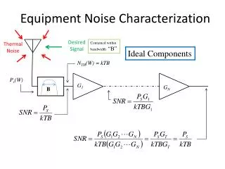
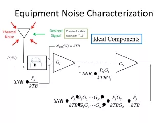
Project Overview • Noise Measurements of Thin-Film Devices on Glass is necessary for understanding their operation and modeling their behavior • Many noise measurements are required to accurately model any new technology • 1/f Noise measurements take a long time due to extremely low frequencies (1 mHz) • Devices under test must be accurately biased for the entire duration
Project Overview • Design & build an automated low noise measurement environment • Computer-Controlled Low noise biasing • Low noise signal amplification • Interface with and unify operation of laboratory measurement apparatus • Lower budget than competing commercial solutions • Cascade Microtech EDGE 1/f Noise Management System: • $1.2 million, but has more functionality • Thermal Chuck, Automated Probers, Automated Data Analysis, Higher Bandwidth, etc. • Aimed at commercial foundries improving process for marketing high-performance silicon • ADIML VIKING Platform • Approximately $1,000 • “Bare bones” automated noise measurements • Aimed at low budget research groups for characterization, rather than production testing
Customer Needs • EMI/RFI Shielded Environment • Localized, low noise amplification of DUT noise signal • Low noise, programmable DC biasing of DUT • Immunity from 60Hz AC power interference • Full noise measurement cycle is software-controllable • IV Sweep Device Bias Noise Measurement Data Acquisition • Interface with existing wafer probe station • Maintain full movement of wafer chuck and microscope gantry • Maintain view of wafer during measurement; RF shielding must remain • System must operate for several hours at a time • No clocks or oscillators inside shielded environment
Specifications - Problems • Issue with current bias circuit prevents circuit from settling. • Recent simulations show this can be fixed easily • Drain bias current resolution not yet measurable: • Nano- or pico-ammeter not available, still developing a measurement circuit using LNA to amplify current • LNA has an offset voltage that affects results at high gain settings • Battery life untested. • 9V batteries purchased could not output enough current for the circuit • Need to purchase new batteries
Analog Circuitry – Voltage Bias Circuitry • Control Voltage comes from a DAC located on the PCB. • RFilter & C form a LPF with corner frequency of 1mHz. • >60dB attenuation of noise in the measurement frequency range, 1Hz to 100kHz • RCharge allows for capacitor to reach desired voltage levels quickly.
Resistor-Based Current Bias Generation • Uses battery and resistor, or op-amp biasing scheme to produce a fixed voltage across a resistor • Fundamentally limited in noise performance • Resistor thermal noise floor of RD Image: Kwok K. Hung, et. Al. A Physics Based MOSFET Noise Model for Circuit Simulators. IEEE Trans. On Electron Devices. Vol. 37. May 1990.
Analog Circuitry – Current Bias Circuitry • Uses a JFET-based current source • Permits isolation of resistors from output current • Allows resistors to be filtered without attenuating noise at higher frequencies • Circuit topology offers output impedance enhanced by amplifier gain
Analog Circuitry – Current Bias Circuitry Equivalent Noise Model • Use superposition to find contribution of each noise source to output noise current • Choose Cs to attenuate all noise sources appropriately • Assuming large Cs, in1, vn1, inr are made negligible • Amplifier with low vn2 was chosen • JFETs have naturally low in,ch System achieves total output noise current on the order of 100 pA/√Hz
Analog Circuitry – LNA Noise Contribution Noise Analysis of LNA dictates that an amp with a low input voltage noise is chosen Total noise contribution found to be 25 pV/√Hz with AD797 amp
Digital Hardware • Xilinx Coolrunner II CPLD • No internal oscillators • Flexible I/O (Voltage levels, current drive, 33 I/O pins) • Low Cost (< $3) • Familiarity with design environment • Chose Peripherals with Serial Interface • Kept CPLD resource usage low (risk of running out of logic) • Allowed communication protocols to be implemented in software • AD5754BREZ DAC • Maxim MAX1248 ADC • On-Semi AMIS 39101 Relay Drivers • Used a CPLD register for power control lines
Control Software • Developed using LabVIEW • Initial effort at learning the language difficult • Reaping the benefits now (easy maintenance) • Developed highly modular code • Large hierarchy of Virtual Instruments makes high-level modifications easy • Implements peripheral-specific protocols in LabVIEW code • Should make adding additional functionality easier than modifying CPLD hardware or microcontroller firmware • Each register, whether located in the CPLD or a peripheral has a VI which makes setting parameters easy (top level module performs no protocol or bit setting operations) • Easy interface with Dynamic Signal Analyzer and 6501 USB DAQ
Hardware/Software Testing • Initial testing performed without any hardware • Oscilloscope to verify software • Simulations to verify CPLD design • Once PCB arrived and was assembled hardware testing began • Experienced typical hiccups • Verified functionality of CPLD communication and control of power bits • Only design error was an incorrect pinout of JTAG header • Fixed using Xilinx flying leads connector
Schedule • PCB build was delayed several weeks due to several issues: • Soldering was extra work due to lack of solder mask and high component density • Circuit bugs due to schematic entry error (ExpressPCB has no simulator) • Circuit bugs due to design errors • PCB reworks • Full functional/specification testing delayed due to circuit board bugs • Mechanical design delayed due to extracurricular circumstances • On track to be finished very soon
Budget • EMI Enclosure Materials • Metal: $150 • RF Glass and Gasket: $30 • JB Weld: $5 • NI6501A USB DAQ: $100 • Electrical Components: $340 • PC Board: $60, +$100 for final version • Batteries and Charging Solution: $70 • Total: $855 • Not accounted for: • NI LabView License • Xilinx CPLD Programming Cable: $295 • Probe Card: $500 ~ $1000, depending on application
Current Status • Mechanical design fits on probe station and meets all specifications • Scheduled for completion • Still finding bugs in the circuit • Pin-compatible, rail-to-rail amps are available • If that allows the circuit to work, the final PCB can be ordered • Simulations indicate that this was the problem
Digital Hardware / Software Status • CPLD modifications for new relay drivers complete • Including Simulations • Control Software needs updating for new relay drivers • Was pending completion of PCB v2 layout • Need to perform hardware validation of DAC control • DAC has never been soldered to board • Oscilloscope measurements at the right CPLD pins looked correct
References • [1] Johns, David A. and Ken Martin. Analog Integrated Circuit Design. John Wiley and Sons. 1997. • [2] Stanford Research Systems. Model SR570 – Low Noise Current Preamplifer. SRS, Inc. 1997. • [3] Kwok K. Hung, et. Al. A Physics Based MOSFET Noise Model for Circuit Simulators. IEEE Trans. On Electron Devices. Vol. 37. May 1990.
Acknowledgements • Dr. Robert J. Bowman, Faculty Advisor and Principal Investigator • Professor George Slack, Faculty Mentor and Guide