Download
1 / 1
20 likes | 280 Views
CBM. VBM. Quantum Confinement of Crystalline Silicon Nanotubes. Binghai Yan 1 , Gang Zhou 1 , Xiao Cheng Zeng 2 , Bing-Lin Gu 1 , and Wenhui Duan* 1

E N D
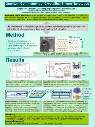
CBM VBM Quantum Confinement of Crystalline Silicon Nanotubes Binghai Yan1, Gang Zhou1, Xiao Cheng Zeng2, Bing-Lin Gu1, and Wenhui Duan*1 1Department of Physics,Tsinghua University, Beijing 100084,China;2Departments of Chemistry and Physics, University of Nebraska, Lincoln, NE 68588,USA Crystalline silicon nanotubes(c-SiNTs),synthesized in experiments recently, are nanotubes of Si crystalline structure with tube-wall-thickness of several nanometers, which are expect to have more advantages to exhibit quantum confinement effect and potential applications than silicon nanowires(SiNWs). Our work studied the electronic, optical and quantum confinement properties of c-SiNTs with both uniform thickness and non-uniform thickness from first-principles. Method Thickness(σ) • Density-functional theory. • The local density approximation. • Norm-conserving pseudopotentials. • Numerical atomic orbitals. • SIESTA package. Diameter TEM image of c-SiNT in experiments (left) and structural model of c-SiNT along [111]: lateral view (middle) and cross section (right). Results Uniform thickness c-SiNTs. The band structure of nanotubes with D=1.80 nm and diffrenet thickness. The band gap increases significantly as the thickness becomes smaller due to quantum confinement. Non-uniform thickness c-SiNTs. The wave-functions of the VBM and CBM are due mainly to atoms located in the thicker side of the tube wall, referred as effective confinement region (ECR). The band gap also depends mainly on ECR. Conduction Channel SEPARATE FET Dopant Impurity For Si nanowires, the dopants will scatter the carriers a lot because the conduction channel and the dopants are in the same position. However, providing the impurity scattering and increasing the conductance is very important to improve the performance of devices, such as FET, For c-SiNTs with non-uniform thickness, the non-uniformity of the VBM and CBM shows a way to spatially separate the doping impurities from the conducting channel in doped SiNTs. Practically, the performance of the SiNT-based transistors may be substantially improved by selective p/n doping in the thinner side of the tube wall, in the spirit of modulation doping. Summary Our study clearly reveals the unique electronic properties of c-SiNTs, especially the effect of non-uniformity in wall thickness, suggesting a new modulation doping method aiming to high-performance nanodevices. Acknowledgement We thank Prof. Jisoon Ihm and Dr. Chaoxing Liu for their helpful discussions.