Download
1 / 2
20 likes | 52 Views
Via, one of the most important components of a PCB, can be plated and crafted in various ways. This blog will let you know the most common types of Vias – through hole, blind hole, buried hole, stub Via, and back-drilled Via.

E N D
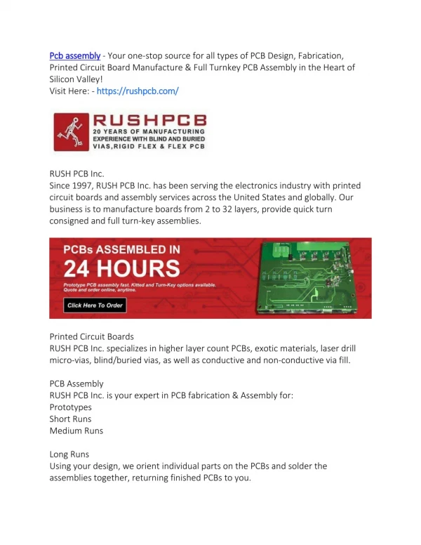
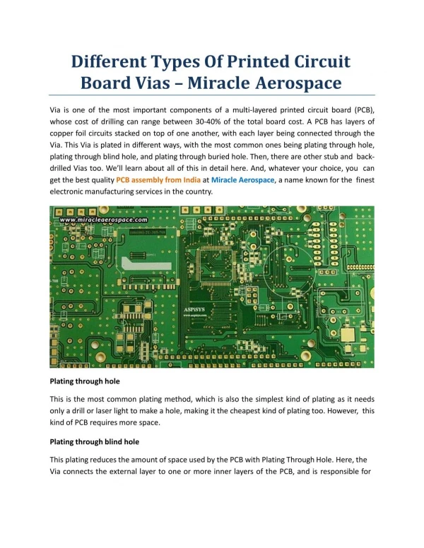
Different Types Of Printed Circuit Board Vias – MiracleAerospace Via is one of the most important components of a multi-layered printed circuit board (PCB), whose cost of drilling can range between 30-40% of the total board cost. A PCB has layers of copper foil circuits stacked on top of one another, with each layer being connected through the Via. This Via is plated in different ways, with the most common ones being plating through hole, plating through blind hole, and plating through buried hole. Then, there are other stub and back-drilled Vias too. We’ll learn about all of this in detail here. And, whatever your choice, you can get the best quality PCB assembly from India at Miracle Aerospace, a name known for the finest electronic manufacturing services in thecountry. Plating throughhole This is the most common plating method, which is also the simplest kind of plating as it needs only a drill or laser light to make a hole, making it the cheapest kind of plating too. However, this kind of PCB requires morespace. Plating through blindhole This plating reduces the amount of space used by the PCB with Plating Through Hole. Here, the ViaconnectstheexternallayertooneormoreinnerlayersofthePCB,andisresponsiblefor
the interconnection between the top layer and inner layers. In this kind of plating, special attention needs to be paid to the depth of the hole. The process of blind hole plating isdifficult. Plating through buriedhole This kind of Via connects to any circuit layer of PCB, but does not pass to the outer layer. This means that only the inner layers of the board are connected by the Via. It is buried inside the board, and not visible from the outside; thus the name. This process of plating is not possible using the method of bonding. Instead, individual circuit layers need to be drilled, and then bound together. Thus, this process requires more time than other processes, which also makes it very expensive. This kind of plating is used in high-density circuit boards as it optimizes the density of the boards without increasing the board size or number of board layersrequired. Stub Via In the stub Via, the through portion starts from the top layer and ends at the inner layer. The stub portion is the remaining portion continuing from the inner layer junction to the bottom layer. Another variation is the through portion originating from one internal signal layer, and terminating on another internal signal layer. Here, there are two stubs – the first stub being from the first internal layer junction to the top layer, and the second stub being from the second internal layer junction to the bottom layer. Back-drilledVia This practice is executed on thick PCBs to minimize stub length for bit-rates greater than 3Gb/s. The process removes the stub portion that is otherwise the case in Plating Through Hole Via. It is a post-fabrication drilling process where the back-drilled hole is of a larger diameter than the original Plating Through Hole. This process can back-drill within 8 mils of the signal layer to keep, so there will always be a small stub portion attached to the Via. However, there are drill bit size and tolerance issues that come with back-drilledVias.