Memory Security Management for FPGA-based Embedded system
Memory Security Management for FPGA-based Embedded system. Russell Tessier, Deepak Unnikrishnan Reconfigurable Computing Group, UMass Amherst, USA tessier@ecs.umass.edu. Romain Vaslin, Guy Gogniat, Jean-Philippe Diguet Lab-STICC CRNS UMR 3192 – UBS Lorient, France vaslin@univ-ubs.fr.

Memory Security Management for FPGA-based Embedded system
E N D
Presentation Transcript
Memory Security Management for FPGA-based Embedded system Russell Tessier, Deepak Unnikrishnan Reconfigurable Computing Group, UMass Amherst, USA tessier@ecs.umass.edu Romain Vaslin, Guy Gogniat, Jean-Philippe Diguet Lab-STICC CRNS UMR 3192 – UBS Lorient, France vaslin@univ-ubs.fr
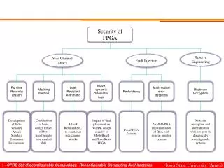
INTRODUCTION • Cost of security: • Memory • Performance • Energy • No architectural trick to solve these issues • New way of building application relying on specific security hardware
OUTLINE • OTP core overview • Security memory management • Experimental approach • Experimental results • Conclusion & future work
OUTLINE • OTP core overview • Security memory management • Experimental approach • Experimental results • Conclusion & future work
OTP core overview (1/4) OTP core principle • Main idea: use the memory acces time to overlap the security computation (OTP generation and integrity checking) • OTP generation: AES core • Integrity checking: CRC
OTP core overview (2/4) Sending data to core Data request Memory answer OTP generation (AES) xor crc (a) Data request Memory answer OTP generation (AES) d1 xor crc d2 xor crc xor crc d3 xor crc d4 xor crc d5 xor crc d6 xor crc d7 xor crc d8 (b) Data request Memory answer OTP generation (AES) xor crc xor crc (c) Data 1-4 Data 5-8 OTP core latency
OTP core overview (3/4) Ciphered cache line Clear cache line OTP CORE : Write request of a cache line AES key Padding value Time Stamp memory Instruction cache AES core @ of Cache line AES core Time Stamp computation AES input AES output External memory Processor core CRC memory CRC generator XOR Data cache TRUSTED ZONE UNTRUSTED ZONE Original OTP core Extended OTP core OTP core architecture – Write request
OTP core overview (4/4) OTP CORE : Read request of a cache line AES key Padding value Time Stamp memory Instruction cache AES core @ of Cache line Time Stamp computation AES input AES output External memory Processor core CRC memory CRC generator Ciphered cache line Clear cache line = ? XOR validation Data cache TRUSTED ZONE UNTRUSTED ZONE Original OTP core Extended OTP core OTP core architecture – Read request
OUTLINE • OTP core overview • Security memory management • Experimental approach • Experimental results • Conclusion & future work
Security memory management (1/4) Uniform protection Non protected Confidentiality Confidentiality / Integrity Principle • Security management based on memory mapping of the code & data • Adapted for application running with an Operating System Task 1 code Task 2 code Task n code OS code R/W data OS data • Advantages: • Reduction of security memory overhead • Reduction of software execution losses • Reduction of power consumption due to security Task 1 stack Task 2 stack Task n stack
Security memory management (2/4) OTP CORE : Read request of a cache line AES key Padding value Time Stamp memory Instruction cache AES core @ of Cache line Time Stamp computation AES input AES output External memory Processor core CRC memory CRC generator Address filtering Ciphered cache line Clear cache line = ? XOR validation Data cache TRUSTED ZONE UNTRUSTED ZONE Original OTP core Extended OTP core Data filtering
Security memory management (3/4) Ciphered cache line Clear cache line Architecture – Write request OTP CORE : Write request of a cache line Security Memory Mapping Core control AES key Task ID Time Stamp memory Instruction cache AES core @ of Cache line AES core Time Stamp computation AES input AES output External memory Processor core CRC memory CRC generator Core control = ? XOR Data cache validation TRUSTED ZONE UNTRUSTED ZONE
Security memory management (4/4) OTP CORE : Read request of a cache line Security Memory Mapping Core control Ciphered cache line Clear cache line AES key Task ID Time Stamp memory Instruction cache AES core @ of Cache line Time Stamp computation AES input AES output External memory Processor core CRC memory CRC generator = ? XOR Data cache validation validation = ? Core control TRUSTED ZONE UNTRUSTED ZONE Architecture – Read request
OUTLINE • OTP core overview • Security memory management • Experimental approach • Experimental results • Conclusion & future work
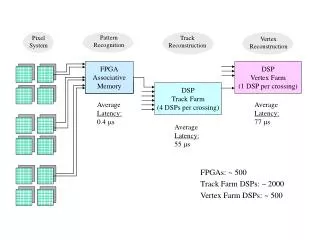
Experimental approach (1/2) Architecture & Applications • Global view of the architecture: • NIOS 2 • High resolution timer • Flash bridge • DDR sdram bridge • JTAG • 4 applications running with MicroC/OS-II: • Image processing (morphological image processing) • Video On Demand (RS, AES, MPEG-2) • Communication (RSd, AES,RSc) • Multi hash (MD5, SHA-1, SHA-2 )
Experimental approach (2/2) Applications partitioning • 3 security levels: • No protection • Uniform protection (Confidentiality & integrity or confidentiality only for the whole memory) • Programmable protection (memory segment & policy decided by the software designer)
OUTLINE • OTP core overview • Security memory management • Experimental approach • Experimental results • Conclusion & future work
Experimental result (1/5) Area overhead Area overhead • Programmable security applied has a direct impact on the size of the design • ~50 % for UP, ~45% for PP • ~65 % for UP, ~70% for PP
Experimental result (2/5) Performances • Software performances losses compared with NP 20.5 % 14.25 % 13.75 % 8.75%
Experimental result (3/5) Memory overhead • Memory overhead is fully dependant of the designer choice for security policy • Memory has a double cost (space & energy) 199.6 kbytes TS data CRC data CRC code 48.8 42.2 43.2 33.2 20 6.8
Experimental result (4/5) No protection Uniform protection Programmable protection Energy consumption 33% 38% 26% 28% ~15% saved compared with UP ~30% saved compared with UP
Experimental result (5/5) No protection Uniform protection Programmable protection Energy consumption 42% 58% 33% 42% ~14% saved compared with UP ~8% saved compared with UP
OUTLINE • OTP core overview • Security memory management • Experimental approach • Experimental results • Conclusion & future work
Conclusion & future work • Security mapping can help to make some save (area, performance, memory, energy) • Fully done in hardware, no OS modification • Dynamic addition of new secured zone • Download of new tasks • Application update/patch • Important difficulties : identification of the entity which is writing in the hardware security core