Download
1 / 9
90 likes | 107 Views
This paper discusses the structure and physics of gated hybrid Hall effect (HHE) devices on silicon. The HHE device features a Si MOSFET with a ferromagnet on top of the gate, which modulates the Hall voltage by changing the direction of magnetization. The device can be integrated with CMOS logic and can interface with Magnetic Quantum Cellular Automata (MQCA) for magnetic storage and processing. Future research directions include shrinking the device dimensions, exploring different magnetic materials, and building nonvolatile memories.

E N D
Gated Hybrid Hall Effect (HHE) devices on silicon Pratyush Das Kanungo, Alexandra Imre, Wu Bin, Alexei Orlov, Greg Snider, Wolfgang Porod Dept of Electrical Engineering, University of Notre Dame Nicholas.P.Carter Dept of Electrical and Computer Engineering, University of Illinois at Urbana Champaign
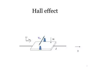
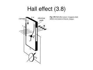
Gated HHE Device – Structure and Physics • Si MOSFET on Si Hall bar • 25nm thick gate oxide,20micron gate length • 20x12micron sized, 150nm thick ferromagnet on top of gate • Hall effect on the 2DEG of inversion channel by the fringing field of ferromagnet • Hall voltage read by passing current through the semiconductor • Hall voltage/resistance changes with the direction of magnetization of the ferromagnet • Binary magnetization states converted into bistable voltage • Change of Hall voltage/resistance modulated by gate bias – effective way of controlling power dissipation Fringing field Ferromagnet Gate 2DEG Si Vg Vg VH+ VH- Change in magnetization direction (M) => Change in sign of Hall voltage (VH+ to VH-) Change in gate voltage (Vg) => Change in magnitude of Hall voltage e- e- M M I I e- e- VH- VH+
HHE device – magnetoelectronic system • Information written as magnetization states by passing a write current through a current line • HIGH, and LOW output Hall voltage according to direction of magntization. • Good remanance in the ferromagnet may lead to hysteresis loop and hence memory • Easily integrated with rest of the CMOS circuit Device structure HHE integrated with CMOS logic
HHE device-interfacing MQCA • Magnetic Quantum Cellular Automata (MQCA) cells can store information • Different magnetic logics can be performed • Can be fabricated on Si substrate at room temperature • HHE device can interface MQCA with CMOS using the same principle of Hall effect • Information can be stored, and processed magnetically, and will be read electrically MQCA Array Spin direction equivalent to logic “0” Spin direction equivalent to logic “1” Proposed device-MQCA interfaced with HHE devie
Fabrication of HHE device-I • Hall Bar defined in thick (240nm) field oxide by image reversal and mesa etch. • Metal (Ti/W) gate defined on top of Hall Bar, and n-wells formed through ion implantation Field oxide P type Si Gate metal Gate oxide n well n well
Fabrication of HHE device-II • Gold bonding pads formed by image reversal and lift-off • Supermalloy deposited on top of the gate by e-beam lithography Metal bond pad n well n well Supermalloy n well n well
Fabricated HHE device, and MQCA at Notre Dame drain Magnetic dot Thirty three antiferromagnetically coupled magnetic dots – MQCA chain I gate drain source 4μ 12μ 10μ Magnet HHE device Magnetic domains in the ferromagnet
Bistable Hall voltage and gate bias modulation • Drop/increase of Hall voltage from HIGH to LOW modulated by gate bias • More gate bias, less Hall voltage/voltage drop/increase, and vice versa HIGH B (external) B (external) VH VH- VH+ I I VH- VH+ LOW Vg Magnet Vg Magnet B
Conclusion, and future direction of research Conclusion • Switching of ferromagnets detected successfully – switching field 150 Gauss • Gate bias modulation of Hall voltage demonstrated Future Research • Shrinking the dimension of HHE device to submicron range • Trying different magnetic material for broader hysteresis loop • Amplifying the output hall voltage • Integrating with MQCA, and fabricate a novel, cost effective, low power magnetoelectronic device on the same silicon substrate • Building nonvolatile memory capable of instant ON operation