Download
1 / 20
220 likes | 549 Views
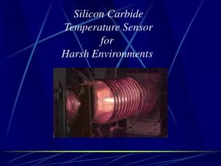
Silicon Carbide Temperature Sensor for Harsh Environments . Team Members. ADVISOR. Chris Rice. Jason Wallace. Dr. Stephen Saddow. “a hot project…a cool advisor”. Michael Jackson. Jovan Bjelobrk. Team Responsibilities. Chris Rice. Sensor Fabrication Sensor Testing. Jason Wallace.

E N D
Silicon Carbide Temperature Sensor for Harsh Environments
Team Members ADVISOR Chris Rice Jason Wallace Dr. Stephen Saddow “a hot project…a cool advisor” Michael Jackson Jovan Bjelobrk
Team Responsibilities Chris Rice • Sensor Fabrication • Sensor Testing Jason Wallace • Documentation • Device Controller • PIC Coding • Software Interface • Device Controller • PIC Coding Michael Jackson • Sensor Fabrication • Sensor Testing Jovan Bjelobrk
Overview • No reliable way to detect temperature changes in extreme environments using typical semiconductor material (Si) • Space travel involves extreme temperatures • SiC has the ability to operate in and withstand extreme temperatures (>500 °C)
Key Specifications • Increased Sensing Range • 25 ° C to 500 ° C • Tolerance • Temperature reading accuracy of 0.5 °C at 25 °C • Cost • Cost of working unit will be less than $300
System Components Temp. Sensor Circuit Software
Fabrication Process • Epitaxial Growth • Photolithography • Metalization • Lift-Off / Etching • Re-Fab • Packaging
Epitaxial Growth n+ n- p+ p+ layer ~ 1019 cm-3 n- layer ~ 5*1015 cm-3 n+ layer ~ 1017 cm-3
Photolithography n+ n- p+
Metalization n+ n- p+
Lift – Off / Etching n- p+ Top View Side View
Design Equations • R = (L/A) • = 1/(qnn) • Ni = sqrt(Nc*Nv)*exp(-Eg/2kT) • n = (2.5*107)*T-2 • A = W*t
L (mm) =100 50 20 10 Resistance vs. Temperature Test Spec of 25 to 500 degrees C
Cost Analysis • ~ $2000 per substrate (2 inch diameter wafer) • ~ $600 for whole-wafer EPI Growth • ~ $400 for Fabrication Run • Producing 24 cells per wafer, and assuming overall yield of process of 72%, produces 120 usable devices at approximately $25 each • Control board components: $26.61 • Total cost for working unit: $51.61
Silicon Carbide Temperature Sensor for Harsh Environments
Demonstration Temperature Center_beta3