Download
1 / 32
340 likes | 630 Views
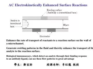
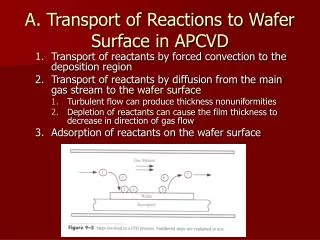
A. Transport of Reactions to Wafer Surface in APCVD. Transport of reactants by forced convection to the deposition region Transport of reactants by diffusion from the main gas stream to the wafer surface Turbulent flow can produce thickness nonuniformities

E N D
A. Transport of Reactions to Wafer Surface in APCVD • Transport of reactants by forced convection to the deposition region • Transport of reactants by diffusion from the main gas stream to the wafer surface • Turbulent flow can produce thickness nonuniformities • Depletion of reactants can cause the film thickness to decrease in direction of gas flow • Adsorption of reactants on the wafer surface
APCVD B. Chemical reaction • Surface migration • Site incorporation on the surface • Desorption of byproducts • Removal of chemical byproducts • Transport of byproduct through the boundary layer • Transport of byproducts by forced convection away from the deposition region
APCVD • At steady state – if two fluxes are equal • The growth rate of the film, v (cm/s), is • Where N is the number of atoms incorporated into the film per unit volume • For single composition film, this is the density
Mole fraction • The mole fraction in incorporating species in the gas phasewhere CT is the concentration of all molecules in the gas phase
Two limiting cases for APCVD model • Surface reaction controlled case (kS<<hG) • Mass transfer or gas-phase diffusion controlled case(hG<<kS)
APCVD • Both cases predict linear growth rates • but they have different coefficients • There is no parabolic growth rate • Surface reaction rate constant is controlled by Arrhenius-type equation (X=Xoe-E/kT) • Quite temperature sensitive • Mass transfer coefficient is relatively temperature independent • Sensitive to changes in partial pressures and total gas pressure
Epitaxial deposition of Si • Slopes of the reaction-limited graphs are all the same • activation energy of about 1.6 eV • This implies the reactions are similar; just the number of atoms is different • There is reason to believe that desorption of H2 from the surface is the rate limiting step • In practice • epitaxial Si at high temperatures (mass transfer regime) • poly-Si is deposited at low temperatures (reaction limited, low surface mobility)
Deposition of Si • Choice of gas affect the overall growth rate • Silane (SiH4) is fastest • SiCl4 is the slowest • Growth rate in the mass transfer regime is inversely dependent on the square root of the source gas molecular weight • Growth rate is dependent on the crystallographic orientation of the wafer • (111) surfaced grow slower than (100) • Results in faceting on nonplanar surfaces
APCVD • In the preceding theory, assumed hG and Cs were constants • Real systems are more complex than this • Consider the chamber where wafers lie on a susceptor (wafer holder). • Stagnant boundary layer, S, is not a constant, but varies along the length of the reactor • Cs varies with reaction chamber length as reaction depletes gases
Effects • Changes the effective cross section of the tube, which changes the gas flow rate • Increasing the flow rate reduces the thickness of the boundary layer and increases the mass transfer coefficient • Reduces gas diffusion length • To correct for the gas depletion effect, the reaction rate is increased along the length of the tube by imposing an increasing temperature gradient of about 5—25oC
APCVD • Sometimes we wish to dope the thin films as they are grown (e.g. PSG, BSG, BPSG, polysilicon, and epitaxial silicon). • Addition of dopants as gases for reaction • AsH3, B2H6, or PH3. • Surface reactions now include • Dissociation of the added doping gases • Lattice site incorporation of dopants • Coverage of dopant atoms by the other atoms in the film
APCVD • Another problem, common in CMOS production, is unintentional doping of lightly doped epitaxial Si when depositing them on a highly doped Si substrate. • Occurs by diffusion because of the high deposition temperatures (800—1000oC) • Growth rate of the deposited layers is usually much faster than diffusion rates (vt >> √Dt), the semi-infinite diffusion model can be applied
Mass transport on to deposited films • Atoms can outgas or be transported by carrier gas from the substrate into the gas stream and get re-deposited downstream • The process is called autodoping • Empirical expression to describe autodoping • C*S is an effective substrate surface concentration and L is an experimentally determined parameter • As film grows in thickness, dopant must diffuse through more film and less dopant enters gas phase.
Autodoping • Autodoping from the backside, edges, or other sources usually results in a relatively constant level. • This is because the source of dopant does not diminish as quickly but is at a much lower level.
APCVD The left part of the curve arises from the out-diffusion from the substrate The straight line part arises from the front-side autodiffusion The background (constant) part is from backside autodoping
In APCVD • It is critical to deliver the same gas flows to all the wafers in order to produce the same growth rates • Wafers placed side-by-side • In LPCVD • Mass transfer coefficient is higher as the diffusion distance of reactants is increased. • the boundary layer thickness slightly increased as P decreases • Reactions are limited by ks where adsorption on wafer surface is key limiting step. • Wafers can be stacked parallel to one another • Note that this arrangement will provide a higher throughput
PECVD • There are some cases where temperature requirements (thermal budget) will not allow high-temperature depositions • E.g., depositing Si3N4 or SiO2 after Al • APCVD and LPCVD do not produce good quality films ~ 450oC • Reaction produced in a plasma ignited using an inert gas between two electrodes • The sample may be heated • Usually between 200-450oC
PECVD • Ideally suited to rapidly varying the film composition and properties during deposition • Apply a potential and an AC signal (13.56 MHz) across a low pressure of the inlet gases • The processes that occur are complicated and very difficult to model • The resultant products are very far from thermodynamic equilibrium • Generates high concentration of particulates • Pinhole density is a problem if chamber is not routinely cleaned.
PECVD Oxide Oxynitride Microfluidic Channels formed by PECVD
CVD LPCVD PECVD
Polysilicon • LPCVD • Deposited by thermal decomposition of silane (SiH4) • Deposition temperature range 580-650°C • SiH4 (vapor) = Si (solid) + 2H2 (gas) • A typical set of deposition parameters: • Temperature: 620°C • Pressure: 0.2-1.0 torr • SiH4 flow rate ~ 250sccm • Deposition rate = 8-10nm/min • Doping of film • In-situ (during deposition) by the addition of dopant gases such as phophine, arsine, and diborane • Often doped after deposition by diffusion or ion implantation • Typically highly doped to achieve low resistance interconnections • 0.01-0.001 ohm-cm can be obtained in diffusion-doped polysilicon.
Silicon dioxide • Variety of methods (PECVD, LPCVD, APCVD) • Index of refraction is used to determine the quality. • Can be doped or undoped • Oxide doped with 5-15% by weight of various dopants can be used as a diffusion source. • PECVD oxide • SiH4 (gas) + 2N2O (gas) SiO2 (solid) + 2N2 (gas) + 2H2 (gas) • Temperature: 200-400°C • Deposition rate of 900nm/min is achievable • Not a good step coverage • Controllable film stress (compressive) • Contains hydrogen (SiOH) • Used for deposition over metals • LPCVD oxide using dichlorosilane • SiCl2H2 + 2N2O SiO2 + 2N2 + 2HCl • Temperatures ~ 900°C • Good step coverage • Compressive stress used to stress-compensate LPCVD nitride
Oxide • LPCVD oxide using tetraethylorthosilicate (TEOS) (liquid source) • Si(OC2H5)4 SiO2 (solid) + 4C2H4 (gas) + 2H2O (gas) • Deposited at temperatures between 650-750°C • Excellent uniformity and step coverage
Silicon nitride • Variety of methods (PECVD, LPCVD, APCVD) • Can be used as an oxidation mask (LPCVD) • An excellent barrier to moisture and sodium contamination (PECVD) • PECVD nitride • SiH4 (gas) + NH3 (gas) SixNyHz (solid) + H2 (gas) • Deposition temperature: 200-400°C • Deposition rate of 20-50nm/min • Not a good step coverage • Controllable film stress • Changes after high temperature anneal due to H2 out-diffusion • LPCVD nitride using dichlorosilane • 2SiCl2H2 (gas) + 4NH3 (gas) Si3N4 (solid) + 6H2 (gas) • Deposition temperatures: 700-800°C • Good step coverage • Tensile stress • Better resistivity (1016 ohm-cm) and dielectric strength (10 MV/cm) compared to PECVD nitride films (106-1015 ohm-cm and 1-5MV/cm)