Download
1 / 22
220 likes | 411 Views
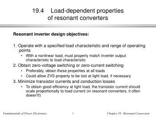
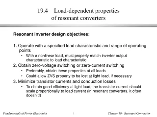
19.4 Load-dependent properties of resonant converters. Resonant inverter design objectives: 1. Operate with a specified load characteristic and range of operating points With a nonlinear load, must properly match inverter output characteristic to load characteristic

E N D
19.4 Load-dependent propertiesof resonant converters • Resonant inverter design objectives: • 1. Operate with a specified load characteristic and range of operating points • With a nonlinear load, must properly match inverter output characteristic to load characteristic • 2. Obtain zero-voltage switching or zero-current switching • Preferably, obtain these properties at all loads • Could allow ZVS property to be lost at light load, if necessary • 3. Minimize transistor currents and conduction losses • To obtain good efficiency at light load, the transistor current should scale proportionally to load current (in resonant converters, it often doesn’t!)
Analysis of inverter output characteristics – simplifying assumptions • Load is resistive • Load does not change resonant frequency • Can include any reactive components in tank • Resonant network is purely reactive (neglect losses)
Inverter output characteristics • Let H be the open-circuit (R→) transfer function: and let Zo0 be the output impedance (with vi→short-circuit). Then, This result can be rearranged to obtain The output voltage magnitude is: Hence, at a given frequency, the output characteristic (i.e., the relation between ||vo|| and ||io||) of any resonant inverter of this class is elliptical. with
with Inverter output characteristics • General resonant inverter output characteristics are elliptical, of the form This result is valid provided that (i) the resonant network is purely reactive, and (ii) the load is purely resistive.
Matching ellipseto application requirements Electronic ballast Electrosurgical generator
Example of gas discharge lamp ignition and steady-state operation from CoPEC research LCC resonant inverter Vg = 300 V Iref = 5 A
Example of repeated lamp ignition attempts with overvoltage protection LCC resonant inverter Vg = 300 V Iref = 5 A Overvoltage protection at 3500 V
19.4 Load-dependent propertiesof resonant converters • Resonant inverter design objectives: • 1. Operate with a specified load characteristic and range of operating points • With a nonlinear load, must properly match inverter output characteristic to load characteristic • 2. Obtain zero-voltage switching or zero-current switching • Preferably, obtain these properties at all loads • Could allow ZVS property to be lost at light load, if necessary • 3. Minimize transistor currents and conduction losses • To obtain good efficiency at light load, the transistor current should scale proportionally to load current (in resonant converters, it often doesn’t!)
Input impedance of the resonant tank networkAppendix C: Section C.4.4 Expressing the tank input impedance as a function of the load resistance R: where
ZN and ZD ZD is equal to the tank output impedance under the condition that the tank input source vs1 is open-circuited. ZD = Zo ZN is equal to the tank output impedance under the condition that the tank input source vs1 is short-circuited. ZN = Zo0
Input impedance of the resonant tank networkAppendix C: Section C.4.4 Expressing the tank input impedance as a function of the load resistance R: where
Magnitude of the tank input impedance If the tank network is purely reactive, then each of its impedances and transfer functions have zero real parts, and the tank input and output impedances are imaginary quantities. Hence, we can express the input impedance magnitude as follows:
A Theorem relating transistor current variations to load resistance R • Theorem 1: If the tank network is purely reactive, then its input impedance || Zi || is a monotonic function of the load resistance R. • So as the load resistance R varies from 0 to , the resonant network input impedance || Zi || varies monotonically from the short-circuit value|| Zi0 || to the open-circuit value || Zi ||. • The impedances || Zi || and || Zi0 || are easy to construct. • If you want to minimize the circulating tank currents at light load, maximize || Zi ||. • Note: for many inverters, || Zi || < || Zi0 || ! The no-load transistor current is therefore greater than the short-circuit transistor current.
Proof of Theorem 1 • Differentiate: • Previously shown: • Derivative has roots at: So the resonant network input impedance is a monotonic function of R, over the range 0 < R < . In the special case || Zi0 ||=|| Zi||,|| Zi || is independent of R.
Example: || Zi|| of LCC • for f < fm, || Zi|| increases with increasing R . • for f > fm, || Zi|| decreases with increasing R . • at a given frequency f, || Zi|| is a monotonic function of R. • It’s not necessary to draw the entire plot: just construct || Zi0|| and || Zi||.
Discussion: LCC LCC example • || Zi0|| and || Zi|| both represent series resonant impedances, whose Bode diagrams are easily constructed. • || Zi0|| and || Zi|| intersect at frequency fm. • For f < fm then || Zi0|| < || Zi|| ; hence transistor current decreases as load current decreases • For f > fm then || Zi0|| > || Zi|| ; hence transistor current increases as load current decreases, and transistor current is greater than or equal to short-circuit current for all R
Discussion —series and parallel • No-load transistor current = 0, both above and below resonance. • ZCS below resonance, ZVS above resonance • Above resonance: no-load transistor current is greater than short-circuit transistor current. ZVS. • Below resonance: no-load transistor current is less than short-circuit current (for f <fm), but determined by || Zi||. ZCS.