Trigger
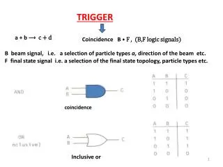
Position offset. Δx. 0.1 mm. Cut on width. mask. Cluster ID. Top Silicon sensor. Communication controler. Coincidence finder (Stub ID). Cluster Width. ~ 1-2 mm. ~ 0.3 mm. Bottom Silicon sensor. Cut on width. mask. Cluster ID. Serial interface (slow control). DAC.

Trigger
E N D
Presentation Transcript
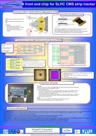
Position offset Δx 0.1 mm Cut on width mask Cluster ID Top Silicon sensor Communication controler Coincidence finder (Stub ID) Cluster Width ~ 1-2 mm ~ 0.3 mm Bottom Silicon sensor Cut on width mask Cluster ID Serial interface (slow control) DAC http://micrhau.in2p3.fr/ A front end chip for SLHC CMS strip tracker • Concept of Silicon strip Pt-module for trigger purpose in sCMS A Pt module for the sCMS silicon tracker • CMS: One of the 4 major experiment of the LHC • Run smoothly with 7Tev pp collision since 2010 • Upgrade : • LHC luminosity to 5x1034cm-2s-1 • Preserve the performance by including the tracker in the level 1 trigger • Local measurement of the particle bending Track stub Track bending in the B-field is inversely proportional to transverse momentum Cluster Width and Offset selection in 2 sensors connected to same Front End ASICs (Pt-module) allows to reject low Pt tracks, reducing band width for read-out of proper trigger information at the LHC clock frequency • Architecture of a pure digital cluster research chip named FEAFS • 2 flows up to the overlap finding • Bus size reduction at each step by priority encoder • Wake up to reduce the power consumption Trigger Wake up Wake up Wake up 64 ampli. 64 discri. 128 strip data Pipeline FIFO Up to 4 clusters 64 inputs from the comparators Threshold cut Priority encoder Cluster Research Up to 32 clusters Up to 32 clusters Up to 6 clusters Up to 12 clusters Overlap finding Priority encoder Strip data Output link MUX FIFO full Up to 6 clusters 64 inputs from the comparators Threshold cut Priority encoder Cluster Research Up to 32 clusters Up to 32 clusters mask thresholds thresholds Slow control FIFO 64 discri. 64 ampli. Strip data Up to 2 clusters Merger Up to 2 clusters 4 inputs from comparators LUT SCL Up to 2 clusters Merger SDA • Algorithm based on a Look Up Table (LUT) • 32 LUTs processes the 128 input strips within one clock cycle • Mergers re-assemble clusters eventually shared by several LUTs Up to 2 clusters 4 inputs from comparators LUT FEAFS chip Up to 2 clusters Merger FULL CHIP 4 inputs from comparators Up to 2 clusters LUT Up to 2 clusters Merger • First prototype developed in 130nm from IBM with approximately 60k VCAD Standard cells • Only 32 inputs : internal demux to regenerate the 128 strips • Size: 4mm² • Sent 31th May 2010 to the foundry • Received from foundry in march 2011. • Mounted in JLCC 68 pins • Test bench and results Test setup: • ASIC test is done by a cyclone IV ALTERA FPGA (on a DE2-115 development board from Terasic) • test control is done either by USB, RS232 or JTAG. • 2 different FPGA firmware : • A random strip generation (with an adjustable probability) is applied on the FEAFS chip. The output bus is compared with an emulated FEAFS design in the FPGA. This firmware is used to test the chip at full speed on a long run period. • A specific pattern written in FPGA ram is applied to the chip. The FEAFS output is recorded for a software analysis. This firmware is used to test the chip at reduce speed on a specific relatively short sequence of strips activity. Results: • Power consumption at 40MHz : 34mA @1.8V = 61.2 mW (60mW expected) • Internal logic is working as expected for a 40 MHz frequency. • Summary and Perspectives • FEAFS first version, was developed to test 130 nm IBM technology with adapted architecture including main digital functionalities and blocks for Strip Pt-modules read-out (Cluster ID and selection, Stub selection, pipeline, FIFO, multiplexer, serial line) but with no specific features to interface to GigaBit Ttansceiver (GBT) system from CERN. • Test results of the chip are in perfect adequacy with simulations. • A new FEAFS version and a “Concentrator” ASIC are now proposed with proper data format and adaptation to the GBT. • Zero suppression and asynchronous read-out can bring a large reduction in number of GBTs, OLs and FEDs. • The FEAFS is the digital part of the front end ASIC, it has to be coupled with an analog part (preamplifier + comparator). Analog part of the CMS Binary Chip (CBC from Imperial College of London) could be a good candidate, but also other developments presented by the pole MICRHAU in the R&D 130nm poster. • More simulation are needed to consolidate evaluation of rates and margins with respect to adaptable parameters and other variables. H. Chanal(1-2), Y. Zoccarato(2-3) (1) LPC Clermont Ferrand, Université Blaise Pascal, CNRS/IN2P3 (2) MICRHAU: pole de MIcroélectronique Rhone, AUvergne (3) Institut de physque nucléaire de Lyon (IPNL), Université de Lyon, Université Lyon 1, CNRS/IN2P3 IN2P3 microelectronic Summer School 2011 -Frejus, 16-19 June 2011