Download
1 / 24
260 likes | 438 Views
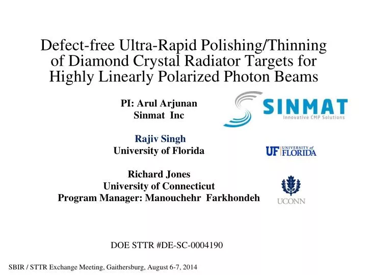
Defect-free Ultra-Rapid Polishing/Thinning of Diamond Crystal Radiator Targets for Highly Linearly Polarized Photon Beams. PI: Arul Arjunan Sinmat Inc Rajiv Singh University of Florida Richard Jones University of Connecticut Program Manager: Manouchehr Farkhondeh. DOE STTR #DE-SC-0004190.

E N D
Defect-free Ultra-Rapid Polishing/Thinning of Diamond Crystal Radiator Targets for Highly Linearly Polarized Photon Beams PI: Arul Arjunan Sinmat Inc Rajiv Singh University of Florida Richard Jones University of Connecticut Program Manager: Manouchehr Farkhondeh DOE STTR #DE-SC-0004190 SBIR / STTR Exchange Meeting, Gaithersburg, August 6-7, 2014
Outline • Application: high-energy polarized photon source • uniqueness of diamond as aradiator • competing specifications:thickness vs. flatness • proposed solution: a thick frame around the radiator • Two approaches investigated • vapor phase ion etching with mask (Sinmat) • milling by UV laser ablation (UConn) • Conclusions and Future Directions SBIR / STTR Exchange Meeting, Gaithersburg, August 6-7, 2014 1
Diamond - a high-energy polarized photon source Radiator Tagger Pair Spectrometer 12 GeV electron beam Crystalline radiator => electrons “bremsstrahlung” from entire planes of atoms at a time • discrete peaks in energy spectrum • photons are polarized within the peaks Diamond is the unique choice for crystal radiator • low atomic number • dense atomic packing • high thermal conductivity • radiation hard, mechanically robust, large-area monocrystals, ... SBIR / STTR Exchange Meeting, Gaithersburg, August 6-7, 2014 2 Coherent Bremsstrahlung 9 GeV polarized photon beam Counting House Photon beam dump Top View 76 m GlueX detector Collimator Electron beam dump
Coherent bremsstrahlung beam properties Bremsstrahlung spectrum with (black) and without (red) an oriented diamond crystal radiator Same spectrum, after cleanup using small-angle collimation SBIR / STTR Exchange Meeting, Gaithersburg, August 6-7, 2014 3
Diamond radiator requirements • thickness 10-4 radiation lengths ~ 20 microns • “mosaic spread” of the crystal planes ~ 20 μrad RMS crystal appears as a mosaic of microscopic quasi-perfect domains • Actually includes other kinds of effects • distributed strain • plastic deformation • Measured directly by X-ray diffraction: “rocking curves” SBIR / STTR Exchange Meeting, Gaithersburg, August 6-7, 2014 4
E6 single-crystal CVD(!) diamond Very close to theoretical rocking curve RMS width for diamond ! but… These crystals are 300 microns thick. X-ray measurements performed at Cornell High Energy Synchrotron Source (CHESS) SBIR / STTR Exchange Meeting, Gaithersburg, August 6-7, 2014 5
E6 CVD diamond thinned to 15 microns Sample was thinned using proprietary Sinmat RCMP process (presented in early talk) • very fragile -- notice the corner broken off • rocking curve shows very large bending deformation (0,1,0) (1,0,0) X-ray measurements performed at Cornell High Energy Synchrotron Source (CHESS) - STTR phase 1 SBIR / STTR Exchange Meeting, Gaithersburg, August 6-7, 2014 6
Primary R&D challenge in Phase 2 Understand and overcome the thin diamond warping problem. Diamonds appear to warp severely when thinned to 20 microns. Try to stiffen the diamond by leaving a thick outer frame around the 20 micron region. Frame around 20 micron window is still part ofthe single crystal, acts like a drum head. Warping is from combination of mounting and internal stresses. SBIR / STTR Exchange Meeting, Gaithersburg, August 6-7, 20147
Two-prong method of attack • Chemical etching using a mask - Sinmat • Step 1: Deposit a metallic mask covering the outer frame region. • Step 2: Etch masked sample using oxygen VPIE. • Monitor removal rates, expect >50 microns/hr • Watch when mask sputters away, when gone return to step 1. • Step 3: Measure central thickness, remove residual mask when done. • 2. Precision milling with a UV laser - UConn • New ablation facility built at UConn for this project • 5W pulsed excimer laser generates 5W at 193nm • UV optics to expand beam, focus to 0.1mm spot • evacuated ablation chamber with tilted sampleholder • 3D motion controls to raster the diamond across thebeam • Software developed to generate smooth flat ablated surface SBIR / STTR Exchange Meeting, Gaithersburg, August 6-7, 2014 8
APPROACH 1: Chemical etching • Slight misalignment shows 4 masks were needed. • Frame thickness is 185 microns • Central region is 55 microns thick • Etched surface shows significant roughness, pits 10 microns deep Careful monitoring needed to prevent burn-through below 50 μm SBIR / STTR Exchange Meeting, Gaithersburg, August 6-7, 2014 9
Vapor Phase Etch Process metal cover mask 2um Al using sputter Diamond • Diamond etching recipe Gases O2 & Ar gas RIE/ICP= 500W / 1500W Diamond 2um Al using Sputter Diamond RIE/ICP etching SBIR / STTR Exchange Meeting, Gaithersburg, August 6-7, 2014
Vapor Phase Etch Process 80um • Etch rate continuously reduced with progressive etching • Al mask re-sputtered on the sample SBIR / STTR Exchange Meeting, Gaithersburg, August 6-7, 2014 11
APPROACH 2: Laser ablation • 200 microns removed in 8hr • surface roughness < 1 μm • risk of burn-through below 50 μm thickness SBIR / STTR Exchange Meeting, Gaithersburg, August 6-7, 2014 12
Uniform sample S90 surface and thickness profiles (Zygo 3D) SBIR / STTR Exchange Meeting, Gaithersburg, August 6-7, 2014 13
Uniform sample S30 Final polish with RCMP technique SBIR / STTR Exchange Meeting, Gaithersburg, August 6-7, 2014 14
X-ray assessment: S90 whole-crystal rocking curve (220) not as flat as S150, but still in spec. SBIR / STTR Exchange Meeting, Gaithersburg, August 6-7, 2014 15
X-ray assessment: S30 rocking curveof S30 Sinmat challenge lies here! SBIR / STTR Exchange Meeting, Gaithersburg, August 6-7, 2014 16
X-ray diffraction: S200_50 352µrad rms result: large bending strain across crystal SBIR / STTR Exchange Meeting, Gaithersburg, August 6-7, 2014 17
X-ray diffraction: UC300_40 surfacewas not treated after ablation excellent result for thinned diamond! SBIR / STTR Exchange Meeting, Gaithersburg, August 6-7, 2014 18
Next steps: large-area 7x7 mm2 • excellent crystal quality • very large thickness 1.2mm SBIR / STTR Exchange Meeting, Gaithersburg, August 6-7, 2014 19
Summary of Methods SBIR / STTR Exchange Meeting, Gaithersburg, August 6-7, 2014 20
Plan: combine the 2 approaches RCMP 30µm removed VPIE 870µm removed 300µm 1.2mm Sent to UConn 330µm Laser Ablation 280µm removed 300µm 20µm SBIR / STTR Exchange Meeting, Gaithersburg, August 6-7, 2014 21
Summary Developed a three-step process to thin diamond samples • Step 1: Vapor phase etching process (75 micron/hr) • Step 2: Polish surface defects with RCMP process • Step 3: Cut thin central window using laser ablation Validated results of all proposed steps using X-ray diffraction • Designed a custom diamond diffraction setup at CHESS • Optimized procedures to obtain 3 rocking curves per hour • Developed analysis code to assess X-ray diffraction topograph • Developed custom analysis code for 2-surface profilometry Expected by Phase 2 completion • 3 production-quality crystals 7x7 mm2 with 20 micron window • draft publication for NP instrumentation journal SBIR / STTR Exchange Meeting, Gaithersburg, August 6-7, 2014 22
Acknowledgements • UConn students • Brendan Pratt (grad) • Igor Senderovich (grad) • FridahMokaya (grad) • Alex Barnes (grad) • Liana Hotte (undergrad) • University of Florida students • Jinhyung Lee (grad) • Jong Cheol Kim (grad) • MinfeiXue (grad) • Nathan Sparks - Catholic University • Ken Finkelstein -CHESS staff and collaborator This work is based upon research conducted at the Cornell High Energy Synchrotron Source (CHESS) which is supported by the National Science Foundation and the National Institutes of Health/National Institute of General Medical Sciences under NSF award DMR-1332208. This work was supported by the United States Department of Energy through STTR award number DE-SC0004190, and by the National Science Foundation through grant number 1207857. SBIR / STTR Exchange Meeting, Gaithersburg, August 6-7, 2014 23