Download
1 / 22
220 likes | 246 Views
Learn about the development of radiation-hard sensors for the ILC forward calorimeter, materials investigated, behavior under radiation, and application in beam monitoring.

E N D
. Radiation hard sensors for ILC forward calorimeter K. Afanaciev Belarus state university CEPC Workshop 2018 IHEP, Beijing
ILC\CLIC Very Forward Region Two calorimeters: LumiCal for Lumi measurement with Bhabha Covers angle ~30 (40) to 80 (100) mrad Two calorimeters: BeamCal for low angle hermeticity. Possibly to estimate beam parameters. Covers angle ~5 (10) to 40 mrad Developed by FCAL collaboration since TESLA
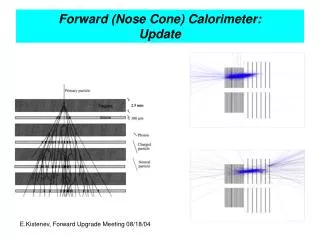
Motivation. ILC\CLIC Very Forward Region EM calorimeter with sandwich structure: 30 layers of 1 X0, 3.5mm W and 0.3mm sensor, Moliére radius RM ≈ 1cm BeamCal From A. Sailer Beamstrahlung (beam-beam interaction) => Coherent and incoherent pairs => Hit BeamCal It is possible to extract some information on beam parameters from pair distribution. See. Ch. Grah and A. Sapronov Beam parameter determination using beamstrahlung photons and incoherent pairs fifth layer Max expected dose about 1 MGy per year of operation (3TeV CLIC), or ~0.5 (ILC). Background from beamstrahlung-generated pairs. Mostly EM, energy ~ 10 MeV (showers). Radiation hard sensors required, cooling is difficult.
Radiation damage Particle knocks atoms out of the crystal lattice – introduces defects These defects could act in different ways Not so important For undoped materials Not so important For wideband materials + surface effects (charge trapping in SiO2) affects electronics
Investigated materials Gallium arsenide (GaAs), Polycrystalline CVD (chemical vapour deposition) Diamond (pCVD) Single crystall CVD Diamond (sCVD) Sapphire . GaAs Si Diamond Sapphire Density 5.32 g/cm3 2.33 3.51 3.98 Pair creation E 4.3 eV/pair 3.6 13 24.6 Band gap 1.42 eV 1.14 5.47 9.9 Electron mobility 8500 cm2/Vs 1350 2200 >600 Hole mobility 400 cm2/Vs 450 1600 - Dielectric const. 12.85 11.9 5.7 9.3-11.5 Radiation length 2.3 cm 9.4 18.8 Ave. Edep/100 m (by 10 MeV e-) 69.7 keV 53.3 34.3 MPV pairs/100 m 15000 7200 3600 2200 Structure p-n or insul. p-n insul. insul.
pCVD Diamond (courtesy of IAF) • pCVD diamond: • radiation hard • Good properties : high mobility, low εR = 5.7, thermal conductivity • availability on wafer scale • Samples investigated: • Element Six(ex-DeBeers) • 1 x 1 cm2 • 200-500 μm thick (typical thickness 300μm) • Ti(/Pt)/Au metallization (courtesy of IAF) The only problem is that there is only one main detector-grade material manufacturer Price is still too high for large-scale application
pCVD Diamond. CCE A number of samples were irradiated (10 MeV electrons) Typical behaviour: Increase in CCD at low dose => pumping - i.e. filling of the traps Then gradual decrease of efficiency with dose @500V After absorbing 7MGy: CVD diamonds still operational. 10 MGy for diamond roughly correspond to 1016 n/cm-2 for Si
pCVD Diamond. Dark current E6_4 sample from Element 6, 500 μm ~ -80% Signal decreased by 80 % after absorbed dose of about 7 MGy Slight increase in dark current, but still in pA range
sCVD Diamond detector Single crystal CVD (chemical vapour deposition) diamond CVD growth on top of diamond substrate +Low defect content, very good detector properties - Small area (up to 5x5mm), very high price Sample produced by Element Six 5x5 mm, 320μm thickness initial charge collection efficiency about 100% (CCD 320μm)
sCVD Diamond. Irradiation results Irradiation to 10 MGy CCE dropped to 10% of the initial value No visible annealing in 18 month No significant increase in the dark current after the irradiation (still in pA range)
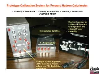
Diamond detector application. CMS beam monitoring Fluence ~ 3x10¹⁴ rough estimate
GaAs Detector Supplied by FCAL group at JINR Produced in Tomsk Sample is semi-insulating GaAs doped by Sn (shallow donor) and compensated by Cr (deep acceptor). This is done to compensate electron trapping centers EL2+ and provide i-type conductivity. Charge transport by electrons only. CCE ~ 50% by default. Sample works as a solid state ionisation chamber Structure provided by metallisation (similar to diamond) 500 m thick detector is divided into 87 5x5 mm pads and mounted on a 0.5mm PCB with fanout Metallisation is V (30 nm) + Au (1 m)
GaAs. Irradiation results. CCE Results: CCE dropped to about 5% from ~50% after 1.5 MGy this corresponds to signal size of about 2000 e- No saturation, signal could be increased with bias voltage
GaAs. Irradiation results. Dark current Dark current increased 2 times (from 0.4 to 1 A @ 200V) Signal is still visible for an absorbed dose of about 1.5 MGy
Sapphire Single crystal Al2O3 grown by Czochralski process Large scale production: crystals up to 500 kg Positive: Cheap, large area, wide bandgap Negative: small response to MIPs (~2200 eh pairs per 100 um) Low charge collection efficiency (~5%) => signal from MIP in Typical 500 um detector ~500 e Courtesy S. Schuwalow
Sapphire Response measured in current mode. Good radiation hardness Dark current ~pA before and after irradiation
Possible application from S. Schuwalow
Silicon. Motivation and who is doing it RD 50 collaboration (www.cern.ch/rd50/ ) since 2003 > 300 members working on radiation hard silicon detectors Goal => Silicon detectors able to withstand fluence up to 1016 1 MeV neutron equivalent per cm-2 (this was demonstrated recently, switch to p-type silicon) New Goal (next 5 years) => Silicon detectors able to withstand fluence up to 1017 1 MeV neutron equivalent per cm-2 (FCC and HL LHC requirements) A working group WODEAN (Workshop on Defect Analysis in Silicon Detectors) RD 50 mostly study strip and pixel detectors. Hadronic irradiation
Silicon. Results overview. Dark current Dark current rises linearly with the fluence RD 50 data This means for 10x10x0.3 mm detector Idark ~ 1 mA @ room temp. => Needs cooling to at least -20C and up to -50C (still uA currents)
Silicon. Results overview. CCE RD 50 data Signal is visible after 1016 n/cm-2, but Vfd goes into kilovolt range Needs at least 1kV bias (no full depletion) and cooling
Silicon. Motivation and who is doing it Similar for CMS