Download
1 / 15
170 likes | 393 Views
ISAT 436 Micro-/Nanofabrication and Applications. Physical Vapor Deposition (PVD) David J. Lawrence Spring 2004. Physical Vapor Deposition (PVD).

E N D
ISAT 436Micro-/Nanofabrication and Applications Physical Vapor Deposition (PVD) David J. Lawrence Spring 2004
Physical Vapor Deposition (PVD) • Physical vapor deposition (PVD) refers to a family of processes in which a material is converted to its vapor phase in a vacuum chamber and condensed onto a substrate surface as a thin film. • PVD can be used to produce coatings of a wide variety of materials: • metals G alloys • ceramics G glasses • semiconductors G polymers
Physical Vapor Deposition (PVD) • All PVD processes consist of the following steps: • synthesis of coating vapor, • vapor transport to the substrate, • condensation of vapors onto the substrate surface to form a thin film. • These steps are carried out inside a vacuum chamber, so evacuation of the chamber always precedes the PVD process.
Physical Vapor Deposition (PVD) • Pressure Units: • 1 atm = 14.7 psia = 29.92 inches Hg • = 760 mm Hg = 760 torr = 1.013 bar • = 1.013 x 10⁵ Pa • 1 Pa = 1 N/m2 = 7.5 x 10⁻³ torr
Physical Vapor Deposition (PVD) • The two most common PVD processes are: • evaporation • sputtering • We have already covered the basics of evaporation. • See pp. 129-134 of Jaeger. • For evaporation, the background pressure in the vacuum chamber is typically ~10-6 Torr (~10-4 Pa) or lower. • For sputtering, the background pressure in the vacuum chamber is typically 10-3 to 10-2 Torr (~1 Pa).
Evaporation • For evaporation, the background pressure in the vacuum chamber is typically ~10-6 Torr (~10-4 Pa) or lower. • A typical vacuum chamber is shown on page 130 of Jaeger. • In order to evaporate a material, it must be heated to a temperature at which its vapor pressure is 10-3 Torr or higher. • E.g., aluminum must be heated to 1000°C or more.
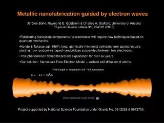
Evaporation • There are two common ways to heat the source material (Jaeger pp. 132-134) : • resistive heating • electron-beam heating. • Resistive heating uses electric current flow through a tungsten filament to heat the source material. • The source material can be placed directly on the tungsten filament, or it can be put in a crucible that is heated by the filament.
Silicon Wafer Aluminum Film Aluminum Vapor Evaporation • Evaporation from a filament-heated crucible.
Evaporation • In electron-beam (e-beam) evaporation systems, a high intensity beam of electrons, with energy up to 15 keV, is focused on the source material. • Electron bombardment heats the source material to the temperature required for evaporation. • Heating can be restricted to the source material itself . Þ The surroundings stay cool. • Because pressure is so low in the vacuum chamber, in evaporation the source material travels in a straight line from the source to the substrate Þshadowing (p. 135 of Jaeger).
Physical Vapor Deposition (PVD) • The mean free path, l of atoms or molecules in a chamber at pressure P is given by • T is the absolute temperature, k is Boltzmann’s constant, and d is the diameter of the gas atoms or molecules • The mean free path is the average distance between collisions in the chamber. • See page 131 of Jaeger.
Physical Vapor Deposition (PVD) • At room temperature and for a typical atom/molecule diameter of 4 Å, the previous equation becomes • The pressure P is in pascals (Pa). • 1 Pa = 1 N/m2 = 7.5 ´ 10-3 Torr • What is the mean free path for typical evaporation and sputtering conditions?
Evaporation • The source material is held on a heated filament, or in a crucible heated by a filament or an electron beam. • The “flux” of atoms evaporating from the surface of the source material is given by: • P is the equilibrium vapor pressure of the source material in Pa (1 Pa = 1 N/m2). • NA is Avogadro’s number = 6.02 x 10²³ particles/mole. • k is Boltzmann’s constant = 1.381 x 10⁻²³ J/K • T is the absolute temperature in °K • M is the atomic mass, converted to kg/mole
Evaporation • The previous equation tells us how many atoms (or molecules) are evaporating from each square meter of the source every second. • The rate of formation of the thin film during evaporation is determined by the impingement rate of these vaporized atoms (or molecules) hitting the substrate surface. • To find the deposition rate of the material on the wafers, we must factor in the area of the source material, the mass of the atoms (or molecules) being deposited, the density of the material being deposited, and the geometry (i.e., what is the wafer position relative to the source material?).
Evaporation • For the simplified case of a wafer directly over the source material, the deposition rate can be reduced to where P, NA , k, T, and M are the same as in the previous equation, and … • As is the area of the source from which atoms are evaporating (in m2) • r is the distance from the source to the wafer (in m), and • r is the density of the deposited material (in kg/m3)
Sputtering • In sputtering, the source material is usually in the form of a sheet or plate, called a target. • Sputtering is achieved by bombarding the target with energetic ions, typically Ar+. • Atoms on the surface of the target are dislodged by this bombardment and fly off . • These atoms then impinge on the substrate, resulting in deposition of a thin film. • See Jaeger (pp. 135-136).