Download
1 / 24
330 likes | 1.01k Views
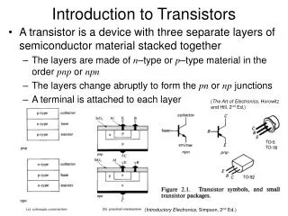
Introduction to Transistors. A transistor is a device with three separate layers of semiconductor material stacked together The layers are made of n –type or p –type material in the order pnp or npn The layers change abruptly to form the pn or np junctions

E N D
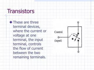
Introduction to Transistors • A transistor is a device with three separate layers of semiconductor material stacked together • The layers are made of n–type or p–type material in the order pnp or npn • The layers change abruptly to form the pn or np junctions • A terminal is attached to each layer (The Art of Electronics, Horowitz and Hill, 2nd Ed.) (Introductory Electronics, Simpson, 2nd Ed.)
Introduction to Transistors • Thus when a transistor is off it behaves like a two–diode circuit • A transistor operates (or turns on) when the base–emitter junction is forward biased and the base–collector junction is reversed biased (“biasing”) (The Art of Electronics, Horowitz and Hill, 2nd Ed.) (Lab 4–1) (Electronic Devices and Circuits, Bogart, 1986)
Transistor Biasing (npn Transistor) • Electrons are constantly supplied to the emitter by the battery with voltage VEE • These electrons can: 1. Recombine with holes in the base, giving rise to IB 2. Diffuse across base and be swept (by electric field at base–emitter junction) into collector, then diffuse around and eventually recombine with holes injected into collector, giving rise to IC • Since the base region is designed so thin, process 2 dominates (no time for #1 to occur as often) • In an actual npn transistor, 98 or 99% of the electrons that diffuse into the base will be swept into the collector
Current Flow Inside a Transistor (Electronic Devices and Circuits, Bogart, 1986) • Current flow for an npn transistor (reverse for pnp): • From conservation of current (IE = IB + IC) we can obtain the following expressions relating the currents: where b≈ 20 – 200 (depends on emitter current) • b increases as IE increases (for very small IE) since there is less chance that recombination will occur in the base • bdecreases slightly (10–20%) as IE increases beyond several mA due to increased base conductivity resulting from larger number of charge carriers in the base • Thus b is not a constant for a given transistor! • An average value of 100 is typically used (and thus IC≈ IE) (Lab 4–5)
Transistor Current Amplification • If the “input” current is IB and the “output” current is IC, then we have a current amplification or gain • Happens because base–emitter junction is forward-biased • Forward bias ensures that the base–emitter junction conducts (transistor is turned on) • Reverse bias ensures that most of the large increase in the base–emitter current shows up as collector current Thus small gains in IB result in large gains in IE and hence IC (Student Manual for The Art of Electronics, Hayes and Horowitz, 2nd Ed.)
(BC junction forward biased) VB VC 0.2 V 0.6 V VE Basic Transistor Switch Circuit (Lab 4–9) • Transistor “switch” circuit: • With switch open, transistor is off and lamp is off • With switch closed, IB = (10 – 0.6) V / 1k = 9.4 mA • However, IC = bIB 940 mA (assuming b = 100) • When collector current IC = 100 mA, lamp has 10V across it • To get a higher current, collector would need to be below ground • Transistor can’t do this, so it goes into saturation • Collector voltage gets as close to emitter voltage as it can (about 0.2 V higher) and IC remains constant (IC is “maxed out”) 0 V (The Art of Electronics, Horowitz and Hill, 2nd Ed.)
(Lab 4–2) Emitter Follower C B • Output “follows” the input: only difference is a 0.6 V diode drop • True for Vin > 0.6 V • If Vin < 0.6 V, transistor turns off (no current – “valve” is closed) and Vout = 0 • Data with RE = 3.3k: E E (The Art of Electronics, Horowitz and Hill, 2nd Ed.) Vin Vout
Emitter Follower • By returning the emitter resistor to a negative supply voltage, you can obtain negative voltage swings as well • Data with RE = 3.3k: (The Art of Electronics, Horowitz and Hill, 2nd Ed.)
Emitter Follower Biasing • You must always provide a DC path for base bias current, even if it is just through a resistor to ground • HW Problem 2.5 (The Art of Electronics, Horowitz and Hill, 2nd Ed.)
Emitter Follower Biasing • With RB included in the previous circuit: f = 1 kHz
Emitter Follower Biasing • Without RB included in the previous circuit: (Here there is no DC base bias current, so transistor is off.)
(Lab 4–4) Emitter Follower Biasing • To obtain symmetric output waveforms without “clipping,” provide constant DC bias using a voltage divider • Capacitors block “outside” DC current, which may affect quiescent (no input) values (“AC-coupled follower”) (The Art of Electronics, Horowitz and Hill, 2nd Ed.)
Emitter Follower Impedance • The usefulness of the emitter follower can be seen by determining its input and output impedance: • Input impedance (i.e. the impedance looking into the base of the transistor): • Details of proof given in class • Output impedance (i.e. the impedance looking into the emitter of the transistor): • Details provided by you in the homework! • Thus the input impedance is much larger than the output impedance
Emitter Follower Impedance • Thus the input and output “sees” what it wants to see on the other side of the transistor: • Using an emitter follower, a given signal source requires less power to drive a load than if the source were to drive the load directly • Very good, since in general we want Zout(stage n) << Zin (stage n + 1) (by at least a factor of 10) • An emitter follower has current gain, even though it has no voltage gain • The emitter follower has power gain (Student Manual for The Art of Electronics, Hayes and Horowitz, 2nd Ed.)
Emitter Follower Impedance • When measuring the input and output impedance of the emitter follower, it is useful to think about the Thévenin equivalent circuit as “seen” at the input and the output: • Input impedance seen by the source: • Output impedance seen by the load: (Lab 4–3) Vin VB Zsource Zin (Student Manual for The Art of Electronics, Hayes and Horowitz, 2nd Ed.) ~ Vout, no load Vout, load Zout Zload
(HW 2.2) Emitter Follower With Load (The Art of Electronics, Horowitz and Hill, 2nd Ed.) Vin IE Vout • Consider the following circuit: • Voutand Vinwaveforms: Vin Vout
Emitter Follower With Load • Thus the npn emitter follower can only “source” current (supply current to something like a load) • It cannot “sink” current (draw current from something like a load) • In this example, the transistor turns off when Vin = –4.4 V(Vout = –5.0 V) • Then IE = 0 and the base–emitter junction becomes reverse biased • As Vin increases further, a rather large reverse bias develops across this junction which could result in breakdown • The output could swing more negative than –5 V by reducing the RE = 1k resistor, but this increases power consumption in both the resistor and transistor
Zener Diodes as Voltage Regulators • Zener diodes “like” to break down at a particular reverse bias: • When reverse biased, they provide a constant voltage drop over a wide range of currents • Zeners thus provide a means of voltage regulation • We choose the specifications for the zener based on: (Student Manual for The Art of Electronics, Hayes and Horowitz, 2nd Ed.) (The Art of Electronics, Horowitz and Hill, 2nd Ed.)
Example Problem 2.3 Design a +10 V regulated supply for load currents from 0 to 100 mA; the input voltage is +20 to +25 V. Allow at least 10 mA zener current under all (worst-case) conditions. What power rating must the zener have? Solution details given in class.
Emitter Followers as Voltage Regulators • However, the zener current can change significantly depending on the load, affecting regulation performance • A better voltage regulator would incorporate an emitter follower: • Here the zener current is more constant, relatively independent of load current since changes in IE (or Iload) produce only small changes in IB • Load current determined from (VB– 0.6 V) / Rload (HW 2.4) (The Art of Electronics, Horowitz and Hill, 2nd Ed.)
Transistors as Current Sources • A transistor can be used as a current source with the setup at right: • Note that IC is independent of VC as long as VC > VE + 0.2 V (i.e., the transistor is not saturated) • The output voltage (Vload orVC) range over which Iload (= IC) is (nearly) constant is called the output compliance (Lab 4–6) VC VE (The Art of Electronics, Horowitz and Hill, 2nd Ed.)
Deficiencies of Current Sources • The load current will still vary somewhat, even when the transistor is “on” and not in saturation • There are two kinds of effects that cause this: • VBEvaries somewhat with collector-to-emitter voltage for a given collector current (Early effect), as does b • DVBE≈ –0.0001 DVCE • We assume VBE = constant = 0.6 V in the basic transistor model • VBE and b depend on temperature • DVBE ≈ –2.1 mV/0C • We neglect changes in b by assuming IC = IE • To minimize DVBEfrom both effects, choose VE large enough ( 1V) so that DVBE 10 mV will not result in large fractional changes in the voltage across RE • VEtoo large will result in decreased output compliance, however (VC range for transistor “on” state decreases)
(Lab 4–7) Common–Emitter Amplifier • Consider a transistor current source with a resistor RC as load, and block unwanted DC at the base input (Vin is an AC signal): so where • Now imagine we apply a base wigglevB via the input signal • The emitter follows the wiggle so vE= vB • Then the wiggle in the emitter current is: (Note DC quiescent output voltage of 10 V) (The Art of Electronics, Horowitz and Hill, 2nd Ed.) (lower-case letters represent small changes, or “wiggles”)
Common–Emitter Amplifier • Now VC = VCC – ICRC so vC= –iCRC = –vB(RC / RE) • Since vin = vB and vout = vC, we have a voltage amplifier, with a voltage gain of: • Minus sign means that a positive wiggle at the input gets turned into a negative wiggle at the output • Input and output impedance: • Zin= R1 R2 bRE ≈ 8k (see figure on previous slide) • Zout = RC (impedance looking into collector) = RC (high Z current source) ≈ RC = 10k (see figure on previous slide) • Be careful to choose R1 and R2 correctly so that design is not b dependent (R1 R2 << bRE)