Download
1 / 14
140 likes | 233 Views
Explore transverse correlation effects and plastic properties in NbSe3 crystals using X-ray microdiffraction, revealing insights into collective dynamics in electronic structures and shear strain. CDW depinning and structural changes are highlighted, emphasizing the impact of crystal thickness variations on CDW structure and transport properties.

E N D
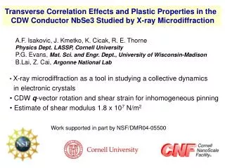
Transverse Correlation Effects and Plastic Properties in the CDW Conductor NbSe3 Studied by X-ray Microdiffraction A.F. Isakovic, J. Kmetko, K. Cicak, R. E. Thorne Physics Dept. LASSP, Cornell University P.G. Evans, Mat. Sci. and Engr. Dept., University of Wisconsin-Madison B.Lai, Z. Cai, Argonne National Lab • X-ray microdiffraction as a tool in studying a collective dynamics • in electronic crystals • CDW q-vector rotation and shear strain for inhomogeneous pinning • Estimate of shear modulus 1.8 x 10⁷ N/m2 Work supported in part by NSF/DMR04-05500
CDW depinning and structural change Most crystals have thickness steps 10mm CDW pinning depends on thickness How do thickness steps/nonuniform pinning affect CDW structure and transport?
Geometry a* c* Previous work: X-ray topography b* t w CDW shear and wavefront deformation due to thickness-dependent pinning
j(mdeg) y (mm) Microdiffraction setup Coherent X-ray beam sample CCD detector zone plate 2j micro- diffraction OSA vertical slits j a* incident beam c* b* diffracted beam Spatial Resolution: 300 nm Sensitivity to Q rotations: 5 mdeg
Sample B, 120 K E = 0 ET step thick 2ET 2.9ET Intensity color scale 3.8ET c* 5 mm 30 m 0 b* Scans in b*-c* plane • Depinning of the thick, weakly pinned • side is accompanied by a loss of • intensity on that side (consistent • with topography experiment) • Spatial resolution is 300 nm • (~ 4 microns in topography) 2 10-3 counts/ monitorcount
thick j y 50 mdeg 2 mm • Most of the effects seen are due to electric field • (zero-field subtracted) • Depinning on the thick side + two types of • rotations (in b*-c* plane and in a-b* plane) • What do we really see in these images? a – b*plane rocking images
C B A 6 mm Individual rocking curves: El. field as parameter • CDW wavevector rotation visible in • curves’ centre-of-mass shift of • 25–40 mdeg • Peak width broadens from the • depinned to pinned side thin thick
0 mm 15 mm Individual rocking curves: lateral position as a parameter
Rotation of CDW q-vector in a - b* plane • Significant rotation of the q-vector in the vicinity of the step • Rotates by 25-40 mdeg, depending on bias and position • Near the step edge region (dj/dy)MAX is ~30 mdeg/mm
FWHM across the step as a function of bias Fitting of the rocking curves • Rotation is pronounced AND • bias dependent across the step • and in the thick region • Rotation in step region occurs in • opposite direction for negative bias
0 mm 15 mm 0 mm 8 mm FWHM: Comparison of samples • Samples with different: • height/thickness ratio • width of the step
Review of some other el./pl. NbSe3 parameters • Consistent picture of longitudinal and transverse properties • Combined X-ray and transport measurements - powerful tool set • Significant differences between the bulk material parameter and • CDW parameter
Shear modulus from both direct readout and fit, we get ~ 30 mdeg/mm Max. shear strain Shear strength Shear modulus Conclusions • X-ray microdiffraction very useful tool in • structural studies of electronic crystals • CDW shear imaged with enhancement • over previous techniques (topograhy) • Rocking curves used to elucidate the • details of the CDW q-vector rotation • Analysis determines the shear strain • modulus G~ 1.8 x 10⁷N/m2 • We also find interesting behavior of the • FWHM in the vicinity of the step edge.
v A hint from raw data: The worst case integrated intensity variations: +/- 10% (between different fields)