Download
1 / 18
200 likes | 965 Views
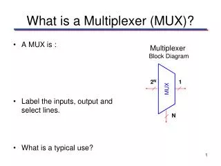
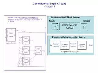
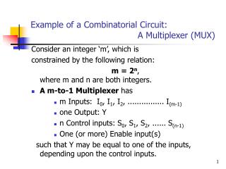
Example of a Combinatorial Circuit: A Multiplexer (MUX). Consider an integer ‘m’, which is constrained by the following relation: m = 2 n , where m and n are both integers. A m-to-1 Multiplexer has

E N D
Example of a Combinatorial Circuit: A Multiplexer (MUX) Consider an integer ‘m’, which is constrained by the following relation: m = 2n, where m and n are both integers. • A m-to-1 Multiplexer has • m Inputs: I0, I1, I2, ................ I(m-1) • one Output: Y • n Control inputs: S0, S1, S2, ...... S(n-1) • One (or more) Enable input(s) such that Y may be equal to one of the inputs, depending upon the control inputs.
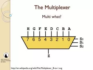
Example: A 4-to-1 Multiplexer A 4-to-1 Multiplexer: I0 I1 Y 2n inputs I2 1 output I3 S0 S1 Enable (G) n control inputs
Characteristic Table of a Multiplexer • If the MUX is enabled, s0 s1 0 0 Y=I0 0 1 Y=I1 1 0 Y=I2 1 1 Y=I3 Putting the above information in the form of a Boolean equation, Y =G. I0. S’1. S’0 +G. I1. S’1. S0 +G. I2. S1. S’0 + G. I3. S1. S0
Implementing Digital Functions: by using a Multiplexer: Example 1 Implementation of F(A,B,C,D)=∑ (m(1,3,5,7,8,10,12,13,14), d(4,6,15)) By using a 16-to-1 multiplexer: I0 0 I1 1 I2 0 I3 1 I4 0 I5 1 I6 F 0 I7 1 I8 1 I9 0 I10 1 I11 0 I12 1 I13 1 I14 1 I15 NOTE: 4,6 and 15 MAY BE CONNECTED to either 0 or 1 0 S3 S2 S1 S0
Implementing Digital Functions: by using a Multiplexer: Example 2 In this example to design a 3 variable logical function, we try to use a 4-to-1 MUX rather than a 8-to-1 MUX. F(x, y, z)=∑ (m(1, 2, 4, 7)
Implementing Digital Functions: by using a Multiplexer: Example 2 ….2 In a canonic form: F = x’.y’.z+ x’.y.z’+x.y’.z’ +x.y.z …… (1) One Possible Solution: Assume that x = S1 , y =S0 . If F is to be obtained from the output of a 4-to-1 MUX, F =S’1. S’0. I0 + S’1. S0. I1 +S1. S’0. I2 + S1. S0. I3 ….(2) From (1) and (2), I0 = I3 =Z I1 = I2 =Z’
Implementing Digital Functions: by using a Multiplexer: Example 2 ….3 Z X Y
Implementing Digital Functions: by using a Multiplexer: Example 2 ….4 Another Possible Solution: Assume that z = S1 , x =S0 . If F is to be obtained from the output of a 4-to-1 MUX, F = S’0 .I0 . S1 +S’0 .I1 . S’1 + S0 .I2 . S’1 +S0 .I3 . S1 ………… (3) From (1) and (2), I0 = y’ = I2 I1 = y = I3
Implementing Digital Functions: by using a Multiplexer: Example 2 ….5
Y0 Y1 Y2 Y4 I0 I1 I2 I3 4 to 1 MUX 1 to 4 DEMUX Y out Input S1 S0 S1 S0 The diagram below shows the relation between a multiplexer and a Demultiplexer.
Demultiplexer (DMUX)/ Decoder A 1-to-m DMUX, with ACTIVE HIGH Outputs, has • 1 Input: I ( also called as the Enable input when the device is called a Decoder) • m ACTIVE HIGH Outputs: Y0, Y1, Y2, ..................................... …………….Y(m-1) • n Control inputs: S0, S1, S2, ...... S(m-1)
Characteristic table of the 1-to-4 DMUX with ACTIVE HIGH Outputs: Table 2
Characteristic Table of a 1-to-4 DMUX, with ACTIVE LOW Outputs: Table 3
Y0 Y1 Y2 Y4 2 to 4 Decoder ENABLE INPUT S1 S0 A Decoder is a Demultiplexer with a change in the name of the inputs : When the IC is used as a Decoder, the input I is called an Enable input
DECODER: In Tables 2 and 3, when Enable is 0, i.e. when the IC is Disabled, all the Outputs remain ‘unexcited’. • The ‘unexcited’ state of an Output is 0 for an IC with ACTIVE HIGH Outputs. • The ‘unexcited’ state of an Output is 1 for an IC with ACTIVE LOW Outputs. Enable Input: In a Decoder, the Enable Input can be ACTIVE LOW or ACTIVE HIGH.
Characteristic Table of a 2-to-4 DECODER, with ACTIVE LOW Outputs and with ACTIVE LOW Enable Input: Table 4 Logic expressions for the outputs of the Decoder of Table 4: Y0 = E + S1 + S0 Y1 = E + S1+ S0‘ Y2 = E + S1‘ + S0 Y3 = E + S1‘ + S0‘
A cross-coupled set of NAND gates Characteristic table: X Y Q1 Q2 0 0 1 1 0 1 1 0 1 0 0 1 1 1 For this case, the outputs can be obtained by using the following procedure: (i) Assume a set of values for Q1 and Q2, which exist before the inputs of X = 1 and Y =1 are applied. (ii) Obtain the new set of values for Q1 and Q2 (iii) Verify whether the procedure yields valid results.