How Surface Mount Technology is Applied on PCB
300 likes | 434 Views
Surface mount technology is a component assembly technology related to printed circuit boards. It differs from other PWB methods where the component leads are inserted into plated through-holes and wave-soldered from the bottom to fill in the holes and interconnect the components. It can achieve higher packaging densities, higher reliability, and reduced cost than the plated through-hole insertion process. Currently, surface-mount technology is the process most widely used for low-cost, high-production consumer electronic assemblies. Instead of putting wire leads into holes drilled in the circuit board.components and elements are mounted directly onto the surface of the board in Surface mount technology.<br>

How Surface Mount Technology is Applied on PCB
E N D
Presentation Transcript
The Application of Surface Mount Technology on PCB Surface mount technology is a component assembly technology related to printed circuit boards. It differs from other PWB methods where the component leads are inserted into plated through-holes and wave-soldered from the bottom to fill in the holes and interconnect the components. It can achieve higher packaging densities, higher reliability, and reduced cost than the plated through-hole insertion process. Currently, surface-mount technology is the process most widely used for low-cost, high-production consumer electronic assemblies. Instead of putting wire leads into holes drilled in the circuit board.components and elements are mounted directly onto the surface of the board in Surface mount technology. MOKO TECHNOLOGY https://www.mokotechnology.com/
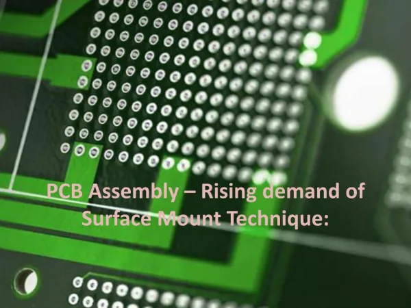
Process of PCB Manufacture Surface mount technology has become the main assembly process of the printed circuit board, which makes the circuit density higher than the single-side or double-side circuit of plated through the hole. The huge majority of today’s electronics are manufactured with Surface-mount technology or surface mount technology. Equipment and products using surface mount technology have many advantages over traditional routing circuits. These devices are called SMDs, or surface mounted devices. These advantages have ensured that Surface mount technology has dominated the PCB world since its conception. 1 3 https://www.mokotechnology.com/ 4
Difference between the through-hole process and surface mount technology When designing a printed circuit board (PCB), one of the first decisions to make is to select the type and style of components to be used. For common component types, such as resistors, capacitors, and diodes, you can usually choose from a variety of available configurations and footprint. The component types selected will influence the size and appearance of the finished printed circuit board assembly (PCBA). https://www.mokotechnology.com/
Difference between the through-hole process and surface mount technology In the past, components with long leads were usually inserted manually into the plated through-hole on the PCB. The leads would then be soldered to form permanent interconnections with the holes. This was known as a through-hole assembly. Increasingly, designers prefer to use a more modern (though by now fully mature) assembly method, which utilizes components whose leads attach to the PCB surface only, without the need for a mating hole. This method was first known as “flat mounting” and later became widely known as surface mounting technology. There are some points that make Surface-mount technology different from Through Hole, which has been briefly listed below; https://www.mokotechnology.com/
Difference between the through-hole process and surface mount technology Surface mount technology has greatly helped solve the common space problems in through-hole mount. The pin count has increased greatly in Surface-mount technology when compared to its older counterparts. In Surface-mount technology, the components are leadless and are directly mounted to the board surface. In the through-hole, the element has leads connected to the wiring board through the through-hole. The Pads on the surface in Surface mount technology are not used for the connection of layers on the printed wiring boards. The components in the Through Hole Technology are larger which leads to lower component density per unit area. The packing density that can be achieved with Surface-mount technology is very high as this allows mounting components on both sides when needed. https://www.mokotechnology.com/
Difference between the through-hole process and surface mount technology Surface mount technology has made possible applications that seemed impossible with through-hole. Surface mount technology is suitable for mass production and can reduce unit assembly cost, which is impossible with through-hole technology. With Surface mount technology, acquiring higher circuit speed is easier due to the reduced size. Surface-mount technology fulfills one of the prime marketing requirements while assisting in making high-performance circuits in a very small size. Surface mount technology has a disadvantage as the capital investment involved in its machinery and production is higher. https://www.mokotechnology.com/
Difference between the surface mount technology and surface mount devices The two acronyms are often confused in electronics manufacturing services. In the paper. They differ by only one letter, but in practice, more SMT and SMD are separate. SMT is the process, and SMD is an abbreviation for surface mount devices, which is one of the components of surface mount technology. Including chips.The SOP.SOJ PLCC.LCCC.OFP, BGA, CSP, FCMCM and so on. Surface-mounted equipment (SMD) is a small part attached to a board in electronics manufacturing. They are designed to be smaller than previous components in response to market demand for smaller, faster and cheaper electronics. Previous components were not only larger but required a different, slower application process. Whereas previous versions of the component had wires running through the circuit board, the pins used in SMD were welded to the circuit board. This means more efficient use of the board space, as there is no need to make holes and both sides of the board become available space.SMDs was created to use efficient and accurate surface mount technology, or surface mount technology https://www.mokotechnology.com/
Aррlісаtіоn оf surface mount technology оn PCB Application of surface mount technology in PCB electronics manufacturing surface mount technology simply means that electronic components are assembled by automated machines that place them on the surface of a board (printed circuit board, PCB).In contrast to traditional through-hole processing (THT), SMT components are placed directly on the surface of the PCB instead of being welded to the conductor.SMT is the most commonly used process in the industry when it comes to electronic assembly. Surface mount technology is almost completely used in PCB assembly and manufacturing. Surface mount technology can encapsulate more electronic components into a smaller space. https://www.mokotechnology.com/
Aррlісаtіоn оf surface mount technology оn PCB Surface mount components are smaller and generally provide better performance levels, and they can be used with automatic pick and place machines, eliminating in many cases the need for manual intervention during assembly. Wire components are also difficult to place automatically because wires need to be pre-formed to fit the relevant hole spacing, and even then they are prone to problems when placed. During PCB assembly, most components on the circuit board are automatically placed. Occasionally, some may require manual intervention, but it has been diminishing. Traditionally, some connectors and other components require auxiliary placement, but the level of6 manual placement has been declining. https://www.mokotechnology.com/
Aррlісаtіоn оf surface mount technology оn PCB Today, printed circuit boards are often developed to minimize this situation or even change the design to use components that can be placed automatically. In addition, component manufacturers have developed a number of specialized surface-mounted versions of components that allow almost complete automated assembly of most circuit boards. Printed circuit boards (PCBs) for surface mount technology (SMT) need to be selected wisely based on factors such as CTE(coefficient of thermal expansion), cost, dielectric performance, and TGA. When designing a surface mount board (PCB), the choice of PCB material is essentially dependent on the type of SMD element used. https://www.mokotechnology.com/
Aррlісаtіоn оf surface mount technology оn PCB In any electronic manufacturing or PCB assembly company, when a lead-free ceramic chip carrier (LCCC) is mounted on a printed circuit board made from a glass epoxy substrate, the solder joint usually cracks about 100 times. The cause of excessive stress is the CTE difference between ceramic packaging and glass epoxy substrate. When designing a surface mount board (PCB), the choice of PCB material is essentially dependent on the type of SMD element used. In any electronic manufacturing or PCB assembly company. When a lead-free ceramic chip carrier (LCCC) is mounted on a printed circuit board made of a glass epoxy substrate, the solder joint usually cracks about 100 times. The cause of excessive stress is the CTE difference between ceramic packaging and glass epoxy substrate. https://www.mokotechnology.com/
Advantages and disadvantages of surface mount technology In the industry. It largely replaced the construction method of through-hole technology, that is, the circuit board with wire components into the hole. Advantages • Miniaturization The geometric size and volume of electronic components in surface mount technology are far smaller than that of through-hole interpolation components. Generally, through-hole interpolation components can be reduced by 60%~70%, and some components can even reduce their size and volume by 90%. Meanwhile, the component weight can be reduced by 60-90%. https://www.mokotechnology.com/
Advantages and disadvantages of surface mount technology High signal transmission speed Surface mount technology assembled components not only the compact structure but also high safety density. When PCB is pasted on both sides, the assembly density can reach 5-5-20 solder joints per square centimeter. SMT PCB can realize high-speed signal transmission due to short circuits and small delays. Meanwhile, SMT assembled PCBs are more resistant to vibration and impact. It is of great significance to realize the ultra-high-speed operation of electronic equipment. • High-frequency effect Because the element has no leads or the leads are short. The distribution parameters of the circuit are reduced and the rf interference is reduced. https://www.mokotechnology.com/
Advantages and disadvantages of surface mount technology Surface mount technology is beneficial to automatic production, improve yield and production efficiency The standardization, serialization, and consistency of the welding conditions of chip components enable the surface mount technology to be highly automated. The failure of components during welding is greatly reduced and the reliability is improved. • Lower material Most SMT components cost less to package than THT components of the same type and function due to increased efficiency of production equipment and reduced consumption of packaging materials. Therefore, the selling price of SMT components is lower than that of THT components. https://www.mokotechnology.com/
Advantages and disadvantages of surface mount technology Simplify production processes and reduce production costs. When installed on the PCB board, there is no need to bend, shape or shorten the lead wire of the components, which shortens the whole process and improves the production efficiency. The processing cost of the same functional circuit is lower than that of the through-hole interpolation, which can generally reduce the total production cost by 30%-50%. https://www.mokotechnology.com/
Advantages and disadvantages of surface mount technology Disadvantages • Small Spaces can make repairs more difficult. • It does not guarantee that the solder joint will withstand the compounds used in the potting process. Connections may or may not be broken when thermal cycling is performed. • Components that generate large amounts of heat or bear high loads should not be surface-mounted because solder melts at high temperatures. • Solder also weakens due to mechanical stress. This means that components that will interact directly with the user should be wired using the physical binding installed through the hole. https://www.mokotechnology.com/
Surface mount assembly process Surface mount technology is the method of attaching electronic components to the surface of PCB. It welds the surface-mount assembly to the plate by reflow soldering. The surface mount assembly process begins at the design stage, where many different components are selected and the PCB is designed using software packages such as Orcad or Capstar. https://www.mokotechnology.com/
Surface mount assembly process Material preparation and inspection Prepare SMC and PCB, check for defects.PCBs usually have flat, usually tin-lead, silver, or gold-plated brazing pads, without holes, called pads. • Template preparation The steel mesh is used for a fixed position in solder paste printing. It is manufactured according to the design position of the pad on the PCB. • Solder paste printing The first machine to be installed during manufacturing is the solder paste printer, which is designed to apply the solder paste to the appropriate solder pad on the PCB using a template and scraper. This is the most widely used method of applying solder paste but spray printing is becoming increasingly popular, especially in sub-contract departments where no template is required and modification is easier to make solder paste, usually flux and a mixture of tin, used to connect SMC and PCB solder pads. It is suitable for PCB and dies using a scraper at 45°-60° Angle solder paste detection. https://www.mokotechnology.com/
Solder paste inspection Most solder paste presses have the option to include automatic detection, but depending on the size of the PCB, this process can be time-consuming, so you can usually choose a separate machine. The internal detection system of the solder paste printer USES 2D technology, while the dedicated SP [machine USES 3D technology for more thorough detection, including the solder paste volume of each pad, not just the print area. Location of components Once the PCB has been confirmed to have the correct number of solder applications, it moves to the next part of the manufacturing process, that is, the placement of the components. Each component is removed from the package with a vacuum or clamping nozzle, checked by the visual system, and placed at a high speed in a programmed position. https://www.mokotechnology.com/
Solder paste inspection First piece inspection (FAI) One of the many challenges subcontractors face is first assembly or first piece inspection (FAI) to verify customer information, which can be time-consuming. This is a very important step in the process because of any error, if undetected, can result in a lot of rework. • Reflow soldering Once all the component positions have been checked, the PCB assembly is transferred to the reflow welder where, by heating the assembly to a sufficient temperature, all the electric welding connections are formed between the component and the PCB. This seems to be one of the less complicated parts of the assembly process, but the correct reflux profile is key to ensuring acceptable solder joints that do not overheat and damage the parts or assembly. https://www.mokotechnology.com/
Solder paste inspection Clean and inspection Clean the board after welding and check for defects. Rework or repair defects and store products. Common SMT related equipment includes magnifying lens, old master (automatic optical inspection), flying needle tester, X-ray machine and other optical inspection machines that can be connected to the machine position so that the component position can be adjusted and SPI machines that can be connected to the printer to allow adjustment of PCB alignment templates. https://www.mokotechnology.com/
Solder paste inspection Solutions to surface mount defects include: • Increase the preheating temperature (in accordance with the recommended guidelines) so that the temperature difference between the terminals is small during reflux.• Select components and PCB boards with consistent solderable leads and pads.• The height of solder paste deposition is measured by the visual system to ensure the same height of solder paste deposition between solder pads.• Inefficient viscous forces are avoided by avoiding extreme environmental conditions• Minimize the amount of movement the assembly sees during reflow.• Increase assembly placement forces to ensure contact between assembly terminals and solder paste deposits (not too much, as a bridge may occur if it is too high). https://www.mokotechnology.com/
MOKO Technology is professional in manufacturing PCB and PCB assembly, with 8 SMT lines, we can assemble 10 million chips per day. MOKO TECHNOLOGY