Download

1 / 30
310 likes | 485 Views
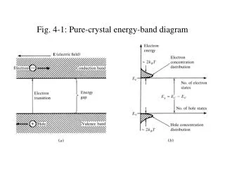
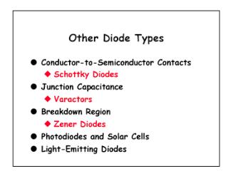
Potential diagram of Schottky barrier (n-type material). Metal. Semiconductor. b. CBM. Fermi-level. VBM. Electrostatics of p++ / n junction or n-Schottky barrier. + + + + + + +. r. d 2 V/dx 2 = - r / e = - q N d /e. E. x=0. E = dV/dx = - r / e dx = - q N d x /e.

E N D
Potential diagram of Schottky barrier (n-type material) Metal Semiconductor b CBM Fermi-level VBM
Electrostatics of p++ / n junction or n-Schottky barrier + + + + + + + r d2V/dx2 = - r/e = - q Nd/e E x=0 E = dV/dx= - r/e dx = - q Nd x/e x=xd -qNdxd/e -V V = - q Nd x/e dx = - q Nd x2 / 2 e
Transition Capacitance of p++ / n junction or n-Schottky barrier i.e. xd = (Vapplied-Vd) 2 e / q Nd PARALLEL PLATE CAPACITOR C = e A / xd CT = A [q Nde / 2 (Vapplied - Vd)]1/2 Vd - Vapplied = - q Nd xd2 / 2 e
Slope o 1/Nd c 1/CT2 = 2 (Vapplied - Vd)/ (q NdeA2) 1/CT2 Vd Vapplied
Slope o 1/Nd 2 c 1/CT2 Slope o 1/Nd 1 c Nd 2 >> Nd 1 Vd Vapplied Nd 2 Nd 1 1/CT2 = 2 (Vapplied - Vd)/ (q NdeA2) Can tailor C(V) by the control of the doping profile, for example for a hyperabrupt junction C is proportional to V-2 facilitating w = (LC)-1/2 being proportional to a control voltage
Diffusion Capacitance of p++ / n junction In forward bias, holes are injected into the n-type region. QD = A q pno Lp (evD/VT - 1) = (Lp2/Dp) I = t I CD = dQ/dV = t dI / dV = t I / (n Vt)