Download
1 / 26
260 likes | 435 Views
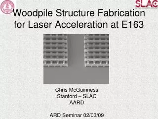
Woodpile Structure Fabrication for Laser Acceleration at E163. Chris McGuinness Stanford – SLAC AARD ARD Seminar 02/03/09. Outline. Gradient Woodpile Structure Fabrication 4 Layer Structure Analysis FTIR Spectroscopy Measurements Simulations Conclusion Where things are at for E163

E N D
Woodpile Structure Fabricationfor Laser Acceleration at E163 Chris McGuinness Stanford – SLAC AARD ARD Seminar 02/03/09
Outline • Gradient • Woodpile Structure Fabrication • 4 Layer Structure Analysis • FTIR Spectroscopy Measurements • Simulations • Conclusion • Where things are at for E163 • Future Experiments
Gradient ?
o Silicon λ=800nm D.M. Simanovskii, et. al. PRL 91 107601 (2003) M. Mero, et. al. Phys. Rev. B 71 115109 (2005) Ben Cowan, Stanford Graduate Thesis (2007) Damage Fluence
Dielectric Accelerator Structures Gratings 3D Photonic Crystal (Woodpile) PBG Fibers Thorlabs HC-1550-2
Accelerating Mode Top View Ratio=1.41 Side View Front View
Gradient 101 SiO2 Eacc=2.76 GV/m @800nm(3.75e5GHZ) ZnS Eacc=1.04 GV/m @5μm(6e4GHZ) Al3O2 Eacc=2.0 GV/m @800nm(3.75e5GHZ) 0 Si Eacc=337 MV/m @1550nm(1.94e5GHZ)
Outline • Gradient • Woodpile Structure Fabrication • 4 Layer Structure Analysis • FTIR Spectroscopy Measurements • Simulations • Conclusion • Where things are at for E163 • Future Experiments
Woodpile Structure • Parameter Scaling* • w=.2757a • h=.3486a • λ=2.703a • Δ=.05a • w=500nm • λ=4.9μm • a=1.814 • h=632nm • Δ=91nm • w=300nm • λ=2.94μm • a=1.09μm • h=379nm • Δ=54nm h w a Δ *Cowan, B. “Photonic Crystal Laser-Driven Accelerator Structures” (PhD dissertation Stanford University 2007) 77.
a w Poly-si 3 Photo resist 5 4 Si Substrate 2 SiO2 1 h SiO2 poly-si SiO2 resist Silicon Substrate Silicon Substrate Fabrication Process Step 1: SiO2 Deposition • Uniformity = 1-2% Step 2: Resist Coat Step 3: Optical Lithography • Minimum feature size 450nm • Alignment 3σ=60nm Step 4: Dry etch SiO2 Step 5: Poly-si Deposition
6 7 8 SiO2 poly-si Frictional Force 10sec=15nm Time Fabrication Process Step 6: Chemical Mechanical Polish Step 7: Repeat process for remaining layers Final Step: Oxide Etch
Completed Four Layer Test Structure October 2008
Outline • Gradient • Woodpile Structure Fabrication • 4 Layer Structure Analysis • FTIR Spectroscopy Measurements • Simulations • Conclusion • Where things are at for E163 • Future Experiments
Finite Thickness SimulationReflection/Transmission(averaged over S&P polarizations, and polar angle θ, φ=0)
SimulationReflection/Transmission(averaged over S&P polarizations, and polar angle θ, φ=0)
Bandgap from MPB Simulation vs. Measurement
Bandgap from MPB Simulation vs. Measurement
Summary • Completed the fabrication of a four layer test structure • Verified a process which will be used for the fabrication of a 15 layer structure with a defect • Taken Spectroscopy measurements • Developed simulation tools that agree well measurements
Current State and Future of E163 • Phase 1: Characterize laser/electron energy exchange in vacuum • Phase 2: Demonstrate optical bunching and acceleration • Phase 3: Test multicell lithographically produced structures
Future Experiments Fabrication • 15 layer structure with defect • Couplers • Focusing Elements Experiments • Wakefield • Measure modes excited by bunched electron beam • Excite defect • Measure mode profile • Measure coupling efficiency • Net Acceleration
Acknowledgments • E163 Collaboration • Bob Siemann, Eric Colby, Chris Sears, Ben Cowan, Joel England, Bob Noble, Jim Spencer • Byer Group • Bob Byer, Tomas Plettner, Alex Serpry, Patrck Liu • NLCTA Operators • Janice Nelson, Doug McCormick • Stanford Nanofab • Mary Tang, Mahnaz Mansourpour, Maurice Stevens, Ed Myers, Uli Thumser, Nancy Latta