Digital Electronics
Digital Electronics. Chapter 5. Synchronous Sequential Logic. SR NAND Latch. Set up the Truth Table. SR NAND Latch. Truth Table. SR NOR Latch. Set up the Truth Table. SR NOR Latch. Truth Table. D Latch.


Digital Electronics
E N D
Presentation Transcript
Chapter 5 Synchronous Sequential Logic
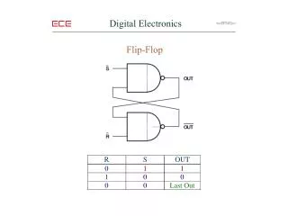
SR NAND Latch Set up the Truth Table
SR NAND Latch Truth Table
SR NOR Latch Set up the Truth Table
SR NOR Latch Truth Table
D Latch Eliminates the indeterminate S=R=1 state of the NAND Latch in addition to a control input C.
Graphic Symbols for Latches Note: 74LS75 is D Latch
Flip-Flops Flip-Flops are triggered by a clock transition in order to make the operation reliable Latch FF FF
Master-Slave D Flip-Flop Master reads while the clock is high but Q records the last data when the clock is low.
Graphic Symbol for 74LS74 Edge-triggered design is superior to master-slave because reading and recording occur in a flash during the clock transition.
T Flip-Flop Determine the Truth Table of the T FF
D Flip-Flop and T Flip-Flop Characteristic Tables D Flip-Flop T Flip-Flop D Q(t+1) T Q(t+1) 0 0 0 No Change 1 1 1 Toggles
Frequency Divider T Flip-Flop can be used to divide the frequency of a clock by 2. Sketch the circuit. How can you divide the frequency by 4?
JK Flip-Flop Draw the Characteristic Table
JK Flip-Flop JK Flip-Flop J K Q(t+1) 0 0 No Change 0 1 0 (reset) 1 0 1(set) 1 1 Toggles
JK Flip-Flop Equation Q(t+1) = JQ' + K'Q 74LS76
What’s wrong with this picture? Connect a wire fom the AND gate to the D Flip-Flop. P.S. This is figure 5-15 in your textbook! P.P.S. Analyze the given sequential circuit. In other words, write the equations for A(t+1), B(t+1), and y, draw a state table, and sketch a state diagram.
State Equations A(t+1) = A x + B x B(t+1) = A' x y = (A + B) x'
State Table Present State Next State Output x = 0 x =1 x = 0 x =1 A B A B A B y y 00 00 01 0 0 01 00 11 1 0 10 00 10 1 0 11 00 10 1 0
Design of Sequential Circuits Design a circuit that detects three or more consecutive 1’s in a string of bits coming through an input line
Planning, Planning, Planning! Our circuit should start off in a “state” S(0). If a 0 comes along it should stay put in S(0). If a 1 comes along it should jump to state S(1). Now if a 0 comes along it should go right back to S(0) but if a second 1 comes along it should jump to S(2). At this point if a third 1 comes along it should jump to S(3) and also set a flag. Otherwise start all over again in S(0).
State Table for Sequence Detector Present State Next State Output x = 0 x =1 x = 0 x =1 A B A B A B y y 00 00 01 0 0 01 00 10 0 0 10 00 11 0 0 11 00 11 1 1
Some Terminology ... FSM:A Sequential Circuit is also called a Finite State Machine (FSM) Mealy Model: The output (y) of an FSM depends on the input (x) as well as the present state of A and B [e.g. Fig 5-15 where y = (A+B)x'] Moore Model: The output (y) of an FSM depends on the present state of A and B but not on the input (x). [e.g. Sequence Detector where y = AB]
VHDL for JK Flip-Flop // Functional description of JK flip-flop module My_JKFlipFlop (J,K,CLK,Q,Qnot); output Q,Qnot; input J,K,CLK; reg Q; assign Qnot = ~ Q ; always @ (posedge CLK) case ({J,K}) 2'b00: Q = Q; 2'b01: Q = 1'b0; 2'b10: Q = 1'b1; 2'b11: Q = ~ Q; endcase endmodule