Download

1 / 18
200 likes | 355 Views
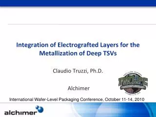
Integration of Electrografted Layers for the Metallization of Deep TSVs. Claudio Truzzi, Ph.D. Alchimer. International Wafer-Level Packaging Conference, October 11-14, 2010. Outline. Introduction: The Drivers for TSVs Limitations of Traditional Dry-Process Approaches

E N D
Integration of Electrografted Layers for the Metallization of Deep TSVs Claudio Truzzi, Ph.D. Alchimer International Wafer-Level Packaging Conference, October 11-14, 2010
Outline • Introduction: The Drivers for TSVs • Limitations of Traditional Dry-Process Approaches • Electrografting Nanotechnology for TSV Applications • Isolation/Barrier/Fill • Isolation and Barrier Film Properties • New Generation TSV Cu Fill • Cost of Ownership • 300-mm Wafer Wet-Process TSV Metallization -Existing Infrastructure • Conclusion
Main 3D-IC Driver • Mobile systems vendors need TSV interconnects to support the bandwidth needed for new data services, which include point-to-point video, a market set to accelerate over the next five years • High-definition video encoding requires about 12.8 GB/s of bandwidth between the processor and DRAM memory • The only way to do that in a mobile system is with TSV-connected logic-memory solution, such as an ARM-based processor stacked with 400 MHz DDR3 memory chips Source: chipdesignmag.com, June 26, 2010
What Type of TSV? • The most strategic question from the design perspective is about aspect ratio • The ability to decrease TSV diameter without affecting wafer thickness has huge implications for how much die space is available for working circuitry, and for the overall cost impact of TSV adoption • At any given wafer thickness, 3DIC designers need TSVs that can be scaled down TSV Area Penalty as a function of AR 12µm 10µm 7µm 5µm 3µm Nominal TSV Diameter • If AR < 10:1 then: • area penalty > 1% • cost >100 USD/wafer
Current TSV Solutions Based on Dry Process + ECD Isolation Cu Seed Cu Fill Barrier Process Step Deposition Methods and Related Issues CVD High Temp>400C Not compatible with memory applications Smooth walls needed -> low etch rate Therm-Oxide Very high temp iPVD/CVD Discontinuous Film AR<10 Inefficient plasma cleaning for AR>5 ALD High Temp>400 C Extremely low UPH High Resistance (i)PVD Poor step coverage AR<10 Discontinuous film Large overburden: thick film on wafer flat to have thin layer on TSV bottom ECD AR<10 Low UPH Size>5µm Strongly acidic Many additives Expensive membrane cells
Dry-Process 300-mm TSV wafer CoOis too high Minimum CapEx (1 tool/step): 70 MUSD Equip. Depr. Cost @ 10 kw/m: 120 USD/wafer Total CoO@ 10 kw/m: 253 USD/wafer
The Way Forward: Scalable Wet-Process TSVs Strong Adhesion • Current wet processing can easily deliver AR>20 at a significantly reduced cost: • Wet Isolation: Polymer-based • Wet Barrier: NiB-based • Cu Fill: directly plated on barrier • Wet Process Properties: • Highly conformal • Strong Adhesion • High Step Coverage • Film properties match or exceed those of dry-processed films High AR Highly Conformal High Step Coverage
Wet Isolation and Barrier Films 10:1 AR 13x133 µm 11:1 AR 9x120 µm 15:1 AR 5x75 µm 18:1 AR 4x72 µm Isolation = 160 nm Barrier = 71 nm Isolation = 130 nm Barrier = 65 nm Isolation = 110 nm Barrier = 48 nm Step coverage : Isolation : 68 % Barrier : 67 %
Wet Isolation - Film properties • CTE falls well within accepted range • Wet Isolation electrical properties match or exceed those of Si02 • Elasticity Modulus and stress values enable the Wet Isolation to play a stress buffer role between Si and Cu
Wet NiB Barrier - Film properties • Resistivity is much lower than industry reference • Barrier properties are equivalent to TiN • Cu diffusion rates equivalent to TaN/Ta • Hardness value is half that of TiN • This is indicative of a less brittle material
High purity Cu fill for narrow, high AR TSVs • Small-diameter high-AR plating capability • High-purity chemistry • Direct plating on Barrier • No chemical degradation of underlying layer • No need for “hot entry” • Seamless integration of complete wet-process TSV Metallization module Cu-fill TSV 2.5X25µm
Contaminants in copper bulk deposited with new fill vs. Baseline ECD chemistry Anneal 250°C • C: 10X less for new fillchemistry • Cl: 100X less for new fillchemistry • S: comparable values Cu bulk Baseline New fill Cl S C S C Cl
Grain size post anneal 400°C underforminggas CommerciallyAvailable New fillChemistry Much higher grain size uniformity Higher grain mean value
Wet Process TSV- Reliability • Successfully passed industry standard reliability tests Wet-Processed TSVs after 1000 temp cycles
Cost of Ownership Model • Assumptions: • 150 kwspy • 300 mm wafer size • 95% process yield • License included • 3 shifts per day • Clean room class: 100 • CR surface ratio: 2,5 • Equipment Depreciation time: 5 years • Maintenance : 3% • CR fully depreciated • via size: 3x30 μ, AR=10 • NEW equipment for etching, deposition (dry, wet), filling $89 Dry $43 $52 eG $18 eG insensitivity to scalloping allows for up to 40µm/min etch rate, contributing to CoO reduction Average savings with Electrografting: 60% Source: Yole Développement
Wet-Process TSV Metallization - 300-mm Wafer Existing Infrastructure • INFRASTRUCTURE • 100m2 class 10K clean room • SEMI complaint consumables and waste treatment • TOOLS • Manual wet benches • ECD cell • SRDs
Wet-Process TSV Metallization - Results Liner Barrier Liner and barrier on Si/SiO2 stack Full stack non-uniformity < 10% Seed
Conclusion • Expensive dry-process tools developed for dual damascene applications are not at home in the TSV world • Integrated, streamlined wet-process solutions are available today delivering higher performance at a significantly reduced cost