Download
1 / 42
480 likes | 925 Views
Ch. 2-1-ARM ARM Instruction Set. ARM instruction set. ARM versions. ARM assembly language. ARM programming model. ARM memory organization. ARM data operations. ARM flow of control. ARM versions. ARM architecture has been extended over several versions.

E N D
ARM instruction set • ARM versions. • ARM assembly language. • ARM programming model. • ARM memory organization. • ARM data operations. • ARM flow of control.
ARM versions • ARM architecture has been extended over several versions. T: Thumb, E: DSP extended, J: JAVA bytecode support • We will concentrate on ARM7.
ARM Core Architecture ;sample prog block 0x1000 LDR R0, [R4, R5] 0x1004 LDR R1, [R4, #8] 0x1008 ADD R2, R0, #5 0x100C SUB R3, R1, R2 0x1010 STR R3, [R2, #4] IA[31:0] ID[31:0] I. Address Register Instruction Decoder PC +4 Control Control Signal Register Bank PC Data In Register ALU Bus C Bus Data out Register Mul’er B Bus A Bus DA[31:0] DD[31:0] Barrel Shifter D. Address Register ALU +1
ARM Processor • ARM Core + Cache, MMU, Write Buffer, TCM, BIU, etc. SoC ARM Processor ARM Core BIU MEM Controler DRAM MMU AMBA Write Buffer FLASH CACHE Virtual Address Physical Address Control Signal Address Data
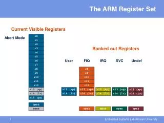
ARM Operation Mode • User Mode • 사용자 테스크를 실행할 때의 모드. 메모리, I/O장치와 같은 시스템 자원의 사용 제한, 비특권모드 • FIQ Mode • 외부 장치 FIQ의 발생 처리 모드 • IRQ Mode • 외부 장치 IRQ의 발생 처리 모드 • SVC (Supervisor) Mode • 커널 혹은 DD를 처리하며, 자유롭게 시스템 자원 사용. Reset 혹은 SWI 발생시 이 모드로 전환하여실행 • Abort Mode • Memory R/W시 오류 발생시에 처리 모드 • Undefined Mode • Fetch한 명령이 정의되어 있지 않는 경우에 오류 처리를 위한 모드 • System Mode • 사용자 모드와 동일. 외부 이벤트에 의해 전환되는 것이 아니라 사용자 프로그램의 필요에 의해 전환되는 모드. 특권모드
ARM General-purpose Register User/System SVC Abort Undefined IRQ FIQ R0 R0 R0 R0 R0 R0 R1 R1 R1 R1 R1 R1 R2 R2 R2 R2 R2 R2 R3 R3 R3 R3 R3 R3 R4 R4 R4 R4 R4 R4 R5 R5 R5 R5 R5 R5 R6 R6 R6 R6 R6 R6 R7 R7 R7 R7 R7 R7 R8 R8 R8 R8 R8 R8_fiq R9 R9 R9 R9 R9 R9_fiq R10 R10 R10 R10 R10 R10_fiq R11 R11 R11 R11 R11 R11_fiq R12 R12 R12 R12 R12 R12_fiq R13_usr R13_svc R13_abt R13_un R13_irq R13_fiq R14_usr R14_svc R14_abt R14_un R14_irq R14_fiq R15(PC) R15(PC) R15(PC) R15(PC) R15(PC) R15(PC) CPSR CPSR CPSR CPSR CPSR CPSR SPSR_svc SPSR_abt SPSR_un SPSR_irq SPSR_fiq
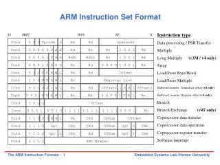
ARM Instruction format Branch Instruction Format Condition Field (4) L: 0=>Branch, 1=>Branch with link Data Processing Instruction Format Condition Field (4) OpCode(4) S: Set Condition Code => 0: unset, 1: set Rn: Source register (4) Rd: Dst register (4) OP2: Immediate 1 OP2: register 0
ARM assembly language • Fairly standard assembly language: LDR r0,[r8] ; a comment label ADD r4,r0,r1
*참고 (MIPS) Preserved on call? no - no no no yes no .- yes yes yes yes
N Z C V ARM programming model r0 r8 r1 r9 0 31 r2 r10 CPSR r3 r11 r4 r12 r5 r13 r6 r14 r7 r15 (PC)
Endianness • Relationship between bit and byte/word ordering defines endianness: Word 8 Word 4 byte 3 byte 2 byte 1 byte 0 byte 0 byte 1 byte 2 byte 3 Word 0 little-endian big-endian The lowest-order byte stored in the low-order bits of the word The lowest-order byte stored in the high-order bits of the word “1234” ? “1234” ?
Strings in real memory • Place strings (and other data) in “data segment”.text add $t0,$s1,$s2 # assembly instructions .data astring: .asciiz “Thisis a string” # data • Assembler keeps track of label addresses • Memory layout: “Big-endian” vs. “Little-endian” address ‘\0’ ‘g’ ‘n’ ‘i’ ‘r’ ‘t’ ‘s’ ‘a’ ‘s’ ‘i’ Astring:0x04001000 ‘s’ ‘i’ ‘h’ ‘T’ Big-Endian
ARM data types • Word is 32 bits long. • Word can be divided into four 8-bit bytes. • ARM addresses can be 32 bits long. • Address refers to byte. • Address 4 starts at byte 4. • Can be configured at power-up as either little- or bit-endian mode.
ARM status bits • Every arithmetic, logical, or shifting operation sets CPSR bits: • N (negative), Z (zero), C (carry), V (overflow). • Examples: • -1 + 1 = 0: NZCV = 0110. • 0 – 1 = -1: NZCV = 1000. • (231-1)+1 = -231: NZCV = 1001. 0xffffff + 0x1 0 + 0xffffff 0x7fffff + 0x1
ARM data instructions • Basic format: ADD r0,r1,r2 • Computes r1+r2, stores in r0. • Immediate operand: ADD r0,r1,#2 • Computes r1+2, stores in r0.
ADD, ADC : add (w. carry) SUB, SBC : subtract (w. carry) RSB, RSC : reverse subtract (w. carry) MUL, MLA : multiply (and accumulate) AND, ORR, EOR BIC : bit clear LSL, LSR : logical shift left/right ASL, ASR : arithmetic shift left/right ROR : rotate right RRX : rotate right extended with C ARM data instructions
Data operation varieties • Logical shift: • fills with zeroes. • Arithmetic shift: • fills with a sign bit if shift right. • Fills with a zero if shift left • RRX performs 33-bit rotate, including C bit from CPSR above sign bit.
ARM comparison instructions • CMP : compare • CMN : negated compare • TST : bit-wise AND • TEQ : bit-wise XOR * These instructions set only the NZCV bits of CPSR.
ARM move instructions • MOV, MVN : move (negated) MOV r0, r1 ; sets r0 to r1
ARM load/store instructions • LDR, LDRH, LDRB : load (half-word, byte) • STR, STRH, STRB : store (half-word, byte) • Addressing modes: • register indirect : LDR r0,[r1] • with second register : LDR r0,[r1,-r2] • with constant : LDR r0,[r1,#4]
ARM ADR pseudo-op • Cannot refer to an address directly in an instruction. • Generate value by performing arithmetic on PC. • ADR pseudo-op generates instruction required to calculate address: ADR r1,FOO
Pseudo-operation ADR ADR r1, FOO 0x201 r15 0x201 SUB r1, r15, #0x101 Distance = 0x101 0x5 0x100 FOO Memory
Example: C assignments • C: x = (a + b) - c; • Assembler: ADR r4,a ; get address for a LDR r0,[r4] ; get value of a ADR r4,b ; get address for b, reusing r4 LDR r1,[r4] ; get value of b ADD r3,r0,r1 ; compute a+b ADR r4,c ; get address for c LDR r2,[r4] ; get value of c SUB r3,r3,r2 ; complete computation of x ADR r4,x ; get address for x STR r3,[r4] ; store value of x
Example: C assignment • C: y = a*(b+c); • Assembler: ADR r4,b ; get address for b LDR r0,[r4] ; get value of b ADR r4,c ; get address for c LDR r1,[r4] ; get value of c ADD r2,r0,r1 ; compute partial result ADR r4,a ; get address for a LDR r0,[r4] ; get value of a MUL r2,r2,r0 ; compute final value for y ADR r4,y ; get address for y STR r2,[r4] ; store y
Example: C assignment • C: z = (a << 2) | (b & 15); • Assembler: ADR r4,a ; get address for a LDR r0,[r4] ; get value of a MOV r0,r0,LSL 2 ; perform shift ADR r4,b ; get address for b LDR r1,[r4] ; get value of b AND r1,r1,#15 ; perform AND ORR r1,r0,r1 ; perform OR ADR r4,z ; get address for z STR r1,[r4] ; store value for z
Additional addressing modes • Base-plus-offset addressing: LDR r0,[r1,#16] • Loads from location r1+16 • Auto-indexing increments base register: LDR r0,[r1,#16]! • Post-indexing fetches, then does offset: LDR r0,[r1],#16 • Loads r0 from r1, then adds 16 to r1.
ARM flow of control • All operations can be performed conditionally, testing CPSR: • EQ, NE, CS, CC, MI, PL, VS, VC, HI, LS, GE (N=V), LT (N != V), GT(Z = 0 and N = V), LE (Z = 1 or N != V) • Why N = V if A >= B in CMP A, B? • Just example… • A = 4, B = 3 => N=0, V=0 (C = 1) • A = 3, B = 4 => N=1, V=0 • A = 3, B = 3 => N=0, V=0 • A = (231-1), B = -1 => NZCV = 1001 • Branch operation: B #100 • Add 400 to PC • Can be performed conditionally.
Example: if statement • C: if (a < b) { x = 5; y = c + d; } else x = c - d; • Assembler: ; compute and test condition ADR r4,a ; get address for a LDR r0,[r4] ; get value of a ADR r4,b ; get address for b LDR r1,[r4] ; get value for b CMP r0,r1 ; compare a < b BGE fblock ; if a >= b, branch to false block
If statement, cont’d. ; true block MOV r0,#5 ; generate value for x ADR r4,x ; get address for x STR r0,[r4] ; store x ADR r4,c ; get address for c LDR r0,[r4] ; get value of c ADR r4,d ; get address for d LDR r1,[r4] ; get value of d ADD r0,r0,r1 ; compute y ADR r4,y ; get address for y STR r0,[r4] ; store y B after ; branch around false block
If statement, cont’d. ; false block fblock ADR r4,c ; get address for c LDR r0,[r4] ; get value of c ADR r4,d ; get address for d LDR r1,[r4] ; get value for d SUB r0,r0,r1 ; compute a-b ADR r4,x ; get address for x STR r0,[r4] ; store value of x after ...
Example: Conditional instruction implementation ; true block MOVLT r0,#5 ; generate value for x ADRLT r4,x ; get address for x STRLT r0,[r4] ; store x ADRLT r4,c ; get address for c LDRLT r0,[r4] ; get value of c ADRLT r4,d ; get address for d LDRLT r1,[r4] ; get value of d ADDLT r0,r0,r1 ; compute y ADRLT r4,y ; get address for y STRLT r0,[r4] ; store y
Conditional instruction implementation, cont’d. ; false block ADRGE r4,c ; get address for c LDRGE r0,[r4] ; get value of c ADRGE r4,d ; get address for d LDRGE r1,[r4] ; get value for d SUBGE r0,r0,r1 ; compute a-b ADRGE r4,x ; get address for x STRGE r0,[r4] ; store value of x
Example: switch statement • C: switch (test) { case 0: … break; case 1: … } • Assembler: ADR r2,test ; get address for test LDR r0,[r2] ; load value for test ADR r1,switchtab ; load address for switch table LDR r15,[r1,r0,LSL #2] ; index switch table switchtab DCD case0 DCD case1 … case 0 … ; code for case 0 … case 1 … ; code for case 1 …
Finite Impluse Response (FIR) Filter FIR filter: f = i=1..n cixi f coefficient c1 c4 c2 c3 x1 x2 x3 x4 Sampling data
Example: FIR filter r0 • C: for (i=0, f=0; i<N; i++) f = f + c[i]*x[i]; • Assembler ; loop initiation code MOV r0,#0 ; use r0 for i MOV r8,#0 ; use separate index for arrays ADR r2,N ; get address for N LDR r1,[r2] ; get value of N MOV r2,#0 ; use r2 for f r2 i = 0; f = 0; while (i < N) { f = f + c[i]*x[i]; i++; } r1 r3 r5 r8: index
FIR filter, cont’.d r0 ADR r3,c ; load r3 with base of c ADR r5,x ; load r5 with base of x ; loop body loop LDR r4,[r3,r8] ; get c[i] LDR r6,[r5,r8] ; get x[i] MUL r4,r4,r6 ; compute c[i]*x[i] ADD r2,r2,r4 ; add into running sum ADD r8,r8,#4 ; add one word offset to array index ADD r0,r0,#1 ; add 1 to i CMP r0,r1 ; exit? BLT loop ; if i < N, continue r2 i = 0; f = 0; while (i < N) { f = f + c[i]*x[i]; i++; } r1 r3 r5 r8: index
ARM subroutine linkage • Branch and link instruction: BL foo • Copies current PC to r14. • To return from subroutine: MOV r15,r14
Nested Function calls and stacks void f1(int a) { f2(a); } main f1 void f2(int r) { f3(r, 5); } f2 growth void f3(int x, int y) { g = x + y; } f3 main(a) { f1(xyz); } procedure call stack during execution of f3()
Nested subroutine calls • Nesting/recursion requires coding convention: f1 LDR r0,[r13] ; load arg a (xyz) to f1 into r0 from stack ; set up to call f2() STR r14,[r13, #4]! ; store f1’s return adrs on the stack STR r0, [r13, #4]! ; store arg a to f2 on stack BL f2 ; branch and link to f2 ; return from f1() SUB r13,#4 ; pop f2’s arg off stack LDR r15, [r13], #-4 ; restore register and return Right after calling f1() main’s ret addr Right before calling f2() main’s ret addr Main() main r13 xyz xyz f1’s ret addr f1 r13 a f2 Before BL f2
Summary • Load/store architecture • Most instructions are RISCy, operate in single cycle. • Some multi-register operations take longer. • All instructions can be executed conditionally.