1 / 1

Figure 1. Schematics of Proposed Sub-bandgap Circuit

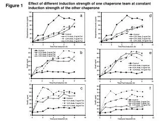
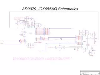
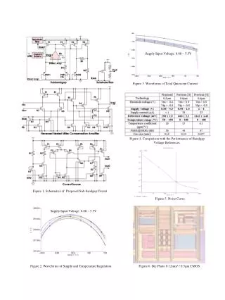
Supply Input Voltage: 0.88 ~ 5.5V. Supply Input Voltage: 0.88 ~ 5.5V. Figure 3. Waveforms of Total Quiescent Current. Figure 4. Comparison with the Performance of Bandgap Voltage References. Figure 1. Schematics of Proposed Sub-bandgap Circuit. Figure 5. Noise Curve.

Download Presentation

Figure 1. Schematics of Proposed Sub-bandgap Circuit

An Image/Link below is provided (as is) to download presentation Download Policy: Content on the Website is provided to you AS IS for your information and personal use and may not be sold / licensed / shared on other websites without getting consent from its author. Content is provided to you AS IS for your information and personal use only. Download presentation by click this link. While downloading, if for some reason you are not able to download a presentation, the publisher may have deleted the file from their server. During download, if you can't get a presentation, the file might be deleted by the publisher.

E N D

Presentation Transcript


  1. Supply Input Voltage: 0.88 ~ 5.5V Supply Input Voltage: 0.88 ~ 5.5V Figure 3. Waveforms of Total Quiescent Current Figure 4. Comparison with the Performance of Bandgap Voltage References. Figure 1. Schematics of Proposed Sub-bandgap Circuit Figure 5. Noise Curve. Figure 2. Waveforms of Supply and Temperature Regulation. Figure 6. Die Photo 0.12mm2 / 0.5m CMOS.

More Related