Download
1 / 44
590 likes | 1.12k Views
Packaging Technologies Trend. Various Packaging Technologies, System On a Chip, System in a Package, Stacked Die Technology, Wafer Level Packaging. VARIOUS PACKAGING TECHNOLOGIES. In Industries Technology can’t make money, low cost make money

E N D
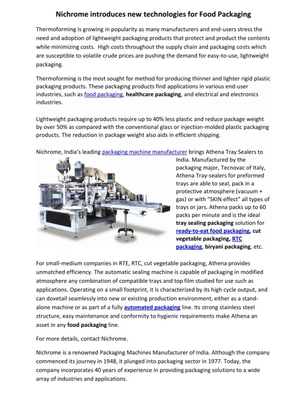
Packaging Technologies Trend Various Packaging Technologies, System On a Chip, System in a Package, Stacked Die Technology, Wafer Level Packaging
In Industries Technology can’t make money, low cost make money PQFP – old technology, most reliable technology, low cost. PBGA – max 5W heat dissipation, end technology FC-BGA /CSP – heat dissipation, as much as we want (use heat sink) DCA-FCOB- most cost effective, no substrate at all, PCB is expensive because of small pitch. So end up, not really a low cost solution WLCSP – with redistribution layer, it make pitch and ball diameter bigger.
SYSTEM ON A CHIP • Definition: Integration of all components into a single chip • Integrating similar technologies provides cost and performance/power advantages • Integrating dissimilar technologies requires balancing cost, process, and functional tradeoffs
SYSTEM ON A CHIP Density, Speed, & Power Consumption are improved… Cost, complexity, and flexibility suffer
SYSTEM IN A PACKAGE • Definition: Integration of all components in/on a single package • Ideal for Integrating functions delivered by dissimilar technologies. • Provides size, flexibility, and performance/power advantages • Will eventually lose to SoC (ie Moore’s Law) when integrating functions implemented in similar technology
SYSTEM IN A PACKAGE • Pragmatic SIP • “Sub-System in a Package”: • Relevant functionality • combined in single package • (e.g. Logic + Memory, RF • etc.) when it makes • business & technical sense • Ultimate SIP • Single multi-function, • package with all needed • system-level functions (e.g. • Analog, Digital, Optical, RF, MEMS)
MANY OPTION OF (SiP) Multi Chip Package Wire Bonded Stacked Die
MANY OPTION OF (SiP) 3D Package Stacking
MANY OPTION OF (SiP) 3D Silicon Stacking
STACKED DIE TECHNOLOGY • With the emergence of mobile electronics and thus the ever increasing of technology integration, IC packaging engineers have to design Multi Chip Packages with the smallest footprint to well compete with System On Chip miniaturization. • This requirement led to the implementation of 3D assembly technology, called stacked die package. Wire bonded stacked die BGA Mixed interconnected stacked BGA
Market Trends • Pyramid Stack. • Intel CSP 4 die stack • 3 mils die • Same Size Stack • STMicroelectronics 4+3 die stack • 50-80µm die • Cross Stack • Intel 8 die stack • 2 mils die
STACKED DIE TECHNOLOGY • Mobile electronic devices use powerful memory capability. • Stacked BGA packages has primarily been developed for integration of memory functions in single package with small footprint. 4Mb SRAM TFBGA 7x7, 48 Balls 49mm2 package surface Stacked BGA TFBGA 8x12, 66 Balls 96mm2 total surface 32Mb SRAM TFBGA 7x12, 48 Balls 84mm2 package surface 4Mb SRAM and 32 Mb Flash stacked die package
0.8mm 1.4mm max 0.3mm THIN WAFER INFRASTRUCTURE • Industry standard for stacked BGA maximum package height is 1.2 to 1.4 mm – very thin wafer must be used. • Wafer thickness requirement 0.18 to 0.25 mm. • Wafer thinning has to be done after wafer bumping since a minimum thickness of 0.55mm is required for the bumping of 200mm wafer. • Specific compliant tape been developed for back grinding of bump wafers (cannot yet reach final thickness of 0.18mm) Cross section of stacked dice BGA
Adhesive film Adhesive paste STACKED DICE BGA - Specific process study Die attach process • Two main approaches used: • Adhesive paste – well known and compatible • Adhesive film – eliminate glue bleeding • Possibilities to use combination of adhesive paste & adhesive film • Limited commercially available system to handle two different wafers forced us to go for double pass die bonding flow Glue cure (snap cure) Glue cure (snap cure) 1st die attach 2nd die attach
Most challenging process for stacked BGA mass production Has to be capable of providing long and short wires with very tight looping control. STACKED DICE BGA - Specific process study Wire Bond process 1
1st kink 2nd kink 3rd kink Upper Die Lower Die STACKED DICE BGA - Challenges Wire Bond process 2 • New loop shape to respect the package thickness requirement has been introduced – long and low loop. • A dedicated “3-kink” loop has been developed. • This new feature has been tested with very positive results with 4mm wire length on top die. • A 160µm loop height has been achieved using this loop shape.
STACKED DICE BGA - Challenges Wire Bond process 3 • In case of higher requirement for loop height reduction, reverse bonding technology can be used. • A 110µm loop height has been reached. • Reduces bonding speed by 40% than the “3-kink” loop process. Standard Bonding Reverse Bonding
REVERSE BONDING The wire is 20µm above die surface Weld bond on stud bump Stacked dice bonding with reverse process
STACKED DIE TECHNOLOGY - Challenges • Due to the need to combine integrated circuits with different form factor, it may happen that the bottom die does not fully support the top die. • A test vehicle was designed with 0.7mm of the die is not supported. A DOE performed to optimize wire bonding parameters for the top die. 0.7mm
OVERHANG : 0.7mm Not supported Risk of poor wire bond on top die
STACKING WITH MIXED TECHNOLOGIES Mixing Flip Chip and Wire bonding • ADVANTAGES • Final mounted heightwith a flip chipinterconnect can be attractive: a small stand-off from bumped die is definitely lower than a wire loop and die attach glue heights. • Simplification of the wire bonding step.
Bumping wafer 1 Backgrinding/Sawing wafer 1 Flip chip Attach Thermosonic or Reflow Die attach wafer 2 Wire bonding wafer 2 PROCESS FLOW – Flip chip + Wire bonding • Specific care should be given to molding that needs to be compatible with low flip chip gap and wire bonds on second die. • This is not an issue when considering Anisotropic Conductive film (ACF) for flip chip attach process because the gap is already filled by the film.
Option 1 Option 2 Bumping wafer FC Bumping wafer FC Backgrinding/Sawing Wafer FC Backgrinding/Sawing Wafer FC Sawing wafer WB Flip Chip attach on WB wafer Die attach lower die on BGA Sawing wafer WB Die attach wafer WB Flip Chip attach on lower die Wire bonding lower die Wire bonding lower die MIX INTERCONNECTIONAssembly flow options Flowcharts of Flip Chips above wire bonded die
WB FC Bumping wafer FC ASSEMBLY FLOW OPTIONS Option 1 Backgrinding / Sawing wafer FC Sawing wafer WB Flip Chip attach on lower die Die attach lower die on BGA Wire bonding lower die
FC ASSEMBLY FLOW OPTIONS Option 2 Flip Chip attach on WB wafer Backgrinding / Sawing wafer FC Bumping wafer FC Wire bonding lower die Die attach wafer WB Sawing wafer WB
MIX INTERCONNECTION (flip chip + wire bond) • This technique supposes that dice are dependant with lower die having a dedicated layout to receive the upper one. • Well matching the Passives and Discretes Integration trend, where these devices can be placed on Silicon substrate and connected to flip chip IC placed above. • A special metalization needs to be applied on the lower die pads, to allow a good interconnect with the bumps.
INTEGRATING PASSIVES AND DISCRETES Flip chip over a NiAu metalized wirebonded die Flip chip reflowed above bonded die
Challenges in dicing thin wafers Lateral Crack on laminated wafer Saw like chipping on bare die Crack at the surface Good interface Step cut solves the problem!! Minor crack line
Pyramid Stack Plasma Cleaning Plasma Cleaning Die Bond / Film Epoxy or paste Die Bond/ Film Epoxy or Paste Oven Cure Oven Cure Top Die Bond Silicon Spacer Bond / Wafer Back Lamination Wire Bonding Wire bond Top Die Bond Wire bond Process Flow Same Size Die Stack
Stack die Materials Thin wafers Stacking options Wire Loop Die Attach 100µm Pyramid Escargot 37 µm 2 die Stack • Ablestik 3230 • Ablestik 5230 • Hitachi HS 230 75µm Bell 44 µm Pyramid + Same size 50µm Ultra Low BSOB 48 µm Mold compound 25µm • Loctite – GR9820 • Sumitomo – G760L • Hitachi – CEL-9220ZHF13 • Shinetsu – KMC 3580 Stack Die
Wafer Thinning Disco Secon Semiconductor • Objective – Thin wafers is key to stacking more dice, hence wafers are targeted to be thinned down to 75 and 50µm • Method • Disco – Dicing Before Grinding (DBG), range of 6 machine, costly and no response in helping us to thin down wafers. • Secon Semi – Atmospheric Downstream Plasma (ADP), already sent out ten 100µm wafers to be thinned to 75 and 50µm..
Die Bond & Wire Bond Challenges Epoxy Film Daughter die Si Spacer Mother die Low loop
Wafer Level Chip Scale Package (WLCSP) One of the unique features of most WLCSPs is the use of a metal layer to redistribute the very fine-pitch peripheral-arrayed pads on the chip of the wafer to much larger-pitch area-arrayed pads with much taller solder joints on the PCB. Advantages: (1) the demand on the PCB is relaxed (2) the PCB assembly of WLCSP is more robust (3) the underfill may not be necessary
Wafer Level (Redistribution) Chip Scale Package Wafer with many chips Chip
What is Wafer Scale Packaging? • Wafer Scale Packing (WSP) can be also be called Wafer Level Packing (WLP) which packages ICs while they are still in wafer form instead of chip form. • WSP includes Wafer Scale Integration (WSI) and Wafer Level Chip Scale Packing (WLCSP). • WLCSP typically replaces conventional die bonding, wire bonding, and encapsulation processes by wafer processing steps such as photo imaging, sputtering and plating. • WLCSP is typically more suitable for devices with less than 150 pin counts due to constraint of the next level of interconnect technology.
Why WLCSP? • Miniaturization - true chip size packaging • Integration - thin film processing enables a high degree of integration • Performance - short lead lengths with controlled dimensions • Shorter cycle time - turn wafer yield excursions from weeks to days; more centralized operations (from fab to assembly to test at one location) • Less testing / handling - test may be carried out only once, at wafer level • Lower cost - potential cost saving due to change of mode of operation (singulation vs. batch), and reduced packaging process steps