Download
1 / 36
360 likes | 506 Views
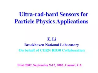
Ultra-rad-hard Sensors for Particle Physics Applications. Li Brookhaven National Laboratory On behalf of CERN RD50 Collaboration. Pixel 2002, September 9-12, 2002, Carmel, CA. RD50 – 271 members.

E N D
Ultra-rad-hard Sensors for Particle Physics Applications • Li • Brookhaven National Laboratory • On behalf of CERN RD50 Collaboration Pixel 2002, September 9-12, 2002, Carmel, CA
RD50 – 271 members J.Adey1, A.Al-Ajili2, P.Alexandrov3, G.Alfieri4, P.P.Allport5, A.Andreazza6, M.Artuso7, S.Assouak8, B.S.Avset9, A.Baldi10, L.Barabash11, E.Baranova3, A.Barcz12, A.Basile13, R.Bates2, B.Bekenov14, N.Belova3, G.M.Bilei15, D.Bisello16, A.Blumenau1, V.Boisvert17, G.Bolla18, V.Bondarenko19, E.Borchi10, L.Borrello20, D.Bortoletto18, M.Boscardin21, L.Bosisio22, G.Bredholt9, L.Breivik9, T.J.Brodbeck23, J.Broz24, A.Brukhanov3, M.Bruzzi10, A.Brzozowski12, M.Bucciolini10, P.Buhmann25, C.Buttar26, F.Campabadal27, D.Campbell23, C.Canali13, A.Candelori16, G.Casse5, A.Chilingarov23, D.Chren24, V.Cindro28, M.Citterio6, R.Coluccia29, D.Contarato25, J.Coutinho1, D.Creanza30, L.Cunningham2, V.Cvetkov3, C.Da Via31, G.-F.Dalla Betta21, G.Davies32, I.Dawson26, W.de Boer33, M.De Palma30, P.Dervan26, A.Dierlamm33, S.Dittongo22, L.Dobrzanski12, Z.Dolezal24, A.Dolgolenko11, J.Due-Hansen9, T.Eberlein1, V.Eremin34, C.Fall1, C.Fleta27, E.Forton8, S.Franchenko3, E.Fretwurst25, F.Gamaz35, C.Garcia36, J.E.Garcia-Navarro36, E.Gaubas37, M.-H.Genest35, K.A.Gill17, K.Giolo18, M.Glaser17, C.Goessling38, V.Golovine14, J.Goss1, A.Gouldwell2, G.Grégoire8, P.Gregori21, E.Grigoriev14, C.Grigson26, A.Groza11, J.Guskov39, L.Haddad2, R.Harding32, J.Härkönen40, J.Hasi31, F.Hauler33, S.Hayama32, F.Hönniger25, T.Horazdovsky24, R.Horisberger41, M.Horn2, A.Houdayer35, B.Hourahine1, A.Hruban12, G.Hughes23, I.Ilyashenko34, A.Ivanov34, K.Jarasiunas37, R.Jasinskaite37, T.Jin32, B.K.Jones23, R.Jones1, C.Joram17, L.Jungermann33, S.Kallijärvi42, P.Kaminski12, A.Karpenko11, A.Karpenko31, A.Karpov14, V.Kazlauskiene37, V.Kazukauskas37, M.Key27, V.Khivrich11, J.Kierstead43, J.Klaiber-Lodewigs38, M.Kleverman44, R.Klingenberg38, P.Kodys24, Z.Kohout24, A.Kok31, A.Kontogeorgakos45, G.Kordas45, A.Kowalik12, R.Kozlowski12, M.Kozodaev14, O.Krasel38, R.Krause-Rehberg19, M.Kuhnke31, A.Kuznetsov4, S.Kwan29, S.Lagomarsino10, T.Lari6, K.Lassila-Perini40, V.Lastovetsky11, S.Latushkin3, R.Lauhakangas46, I.Lazanu47, S.Lazanu47, C.Lebel35, C.Leroy35, Z.Li43, L.Lindstrom44, G.Lindström25, V.Linhart24, A.P.Litovchenko11, P.Litovchenko11, A.Litovchenko16, V.Litvinov3, M.Lozano27, Z.Luczynski12, A.Mainwood32, I.Mandic28, S.Marti i Garcia36, C.Martínez27, S.Marunko39, K.Mathieson2, A.Mazzanti13, J.Melone2, D.Menichelli10, C.Meroni6, A.Messineo20, S.Miglio10, M.Mikuz28, J.Miyamoto18, M.Moll17, E.Monakhov4, L.Murin44, F.Nava13, H.Nikkilä42, E.Nossarzewska-Orlowska12, S.Nummela40, J.Nysten40, R.Orava46, V.OShea2, K.Osterberg46, S.Parker48, C.Parkes2, D.Passeri15, U.Pein25, G.Pellegrini2, L.Perera49, B.Piatkowski12, C.Piemonte21, G.U.Pignatel15, N.Pinho1, S.Pini10, I.Pintilie25, L.Plamu42, L.Polivtsev11, P.Polozov14, J.Popule50, S.Pospisil24, G.Pucker21, V.Radicci30, J.M.Rafí27, F.Ragusa6, M.Rahman2, R.Rando16, K.Remes42, R.Roeder51, T.Rohe41, S.Ronchin21, C.Rott18, A.Roy18, P.Roy2, A.Ruzin39, A.Ryazanov3, S.Sakalauskas37, J.Sanna46, L.Schiavulli30, S.Schnetzer49, T.Schulman46, S.Sciortino10, G.Sellberg29, P.Sellin52, D.Sentenac20, I.Shipsey18, P.Sicho50, T.Sloan23, M.Solar24, S.Son18, B.Sopko24, J.Stahl25, A.Starodumov20, D.Stolze51, R.Stone49, J.Storasta37, N.Strokan34, W.Strupinski12, M.Sudzius37, B.Surma12, A.Suvorov14, B.G.Svensson4, M.Tomasek50, C.Trapalis45, C.Troncon6, A.Tsvetkov24, E.Tuominen40, E.Tuovinen40, T.Tuuva42, M.Tylchin39, H.Uebersee51, J.Uher24, M.Ullán27, J.V.Vaitkus37, P.Vanni13, E.Verbitskaya34, G.Verzellesi13, V.Vrba50, S.Watts31, A.Werner9, I.Wilhelm24, S.Worm49, V.Wright2, R.Wunstorf38, P.Zabierowski12, A.Zaluzhnyi14, M.Zavrtanik28, M.Zen21, V.Zhukov33, N.Zorzi21
RD50 – 52 institutes 1 University of Exeter, Department of Physics, Exeter, EX4 4QL, United Kingdom; 2 Dept. of Physics & Astronomy, Glasgow University, Glasgow, UK; 3 Russian Research Center "Kurchatov Institute", Moscow, Russia; 4 University of Oslo, Physics Department/Physical Electronics, Oslo, Norway; 5 Department of Physics, University of Liverpool, United Kingdom; 6 INFN and University of Milano, Department of Physics, Milano, Italy; 7 Experimental Particle Physics Group, Syracuse University, Syracuse, USA; 8 Université catholique de Louvain, Institut de Physique Nucléaire, Louvain-la-Neuve, Belgium; 9 SINTEF Electronics and Cybernetics Microsystems P.O.Box 124 Blindern N-0314 Oslo, Norway; 10 INFN Florence – Department of Energetics, University of Florence, Italy; 11 Institute for Nuclear Research of the Academy of Sciences of Ukraine, Radiation PhysicDepartments; 12 Institute of Electronic Materials Technology, Warszawa, Poland; 13 Dipartimento di Fisica-Università di Modena e Reggio Emilia, Italy; 14 State Scientific Center of Russian Federation, Institute for Theoretical and Experimental Physics, Moscow, Russia; 15 I.N.F.N. and Università di Perugia – Italy; 6 Dipartimento di Fisica and INFN, Sezione di Padova, Italy; 17 CERN, Geneva, Switzerland; 18 Purdue University, USA; 19 University of Halle; Dept. of Physics, Halle, Germany; 20 Universita` di Pisa and INFN sez. di Pisa, Italy; 21 ITC-IRST, Microsystems Division, Povo, Trento, Italy; 22 I.N.F.N.-Sezione di Trieste, Italy; 23 Department of Physics, Lancaster University, Lancaster, United Kingdom; 24 Czech Technical University in Prague&Charles University Prague, Czech Republic; 25 Institute for Experimental Physics, University of Hamburg, Germany; 26 Experimental Particle Physics Group, Dept of Physics, University of Sheffield, Sheffield, U.K.; 27 Centro Nacional de Microelectrónica (IMB-CNM, CSIC); 28 Jozef Stefan Institute and Department of Physics, University of Ljubljana, Ljubljana, Slovenia; 29 Fermilab, USA; 30 Dipartimento Interateneo di Fisica & INFN - Bari, Italy; 31 Brunel University, Electronic and Computer Engineering Department, Uxbridge, United Kingdom; 32 Physics Department, Kings College London, United Kingdom; 33 University of Karlsruhe, Institut fuer Experimentelle Kernphysik, Karlsruhe, Germany; 34 Ioffe Phisico-Technical Institute of Russian Academy of Sciences, St. Petersburg, Russia; ; 35 Groupe de la Physique des Particules, Université de Montreal, Canada; 36 IFIC Valencia, Apartado 22085, 46071 Valencia, Spain; 37 Institute of Materials Science and Applied Research, Vilnius University, Vilnius, Lithuania; 38 Universitaet Dortmund, Lehrstuhl Experimentelle Physik IV, Dortmund, Germany; 39 Tel Aviv University, Israel; 40 Helsinki Institute of Physics, Helsinki, Finland; 41 Paul Scherrer Institut, Laboratory for Particle Physics, Villigen, Switzerland; 42 University of Oulu, Microelectronics Instrumentation Laboratory, Finland; 43 Brookhaven National Laboratory, Upton, NY, USA; 44 Department of Solid State Physics, University of Lund, Sweden; 45 NCSR DEMOKRITOS, Institute of Materials Science, Aghia Paraskevi Attikis, Greece; 46 High Energy Division of the Department of Physical Science, University of Helsinki, Helsinki, Finland; 47 National Institute for Materials Physics, Bucharest - Magurele, Romania; 48 University of Hawaii; 49 Rutgers University, Piscataway, New Jersey, USA; 50 Institute of Physics, Academy of Sciences of the Czech Republic, Praha, Czech Republic; 51 CiS Institut für Mikrosensorik gGmbH, Erfurt, Germany; 52 Department of Physics, University of Surrey, Guildford, United Kingdom
OUTLINE • Introduction • Radiation induced defects levels in Si • Radiation induced degradation of electrical properties in Si detectors Leakage current Changes in electrical neutral bulk Space charge transformations and CCE loss • RD 50’s approaches to obtain ultra radiation hardness Material /impurity / defect engineering (MIDE) Device structure engineering (DSE) New materials • Future tasks to be carried out by RD 50 • Summary
Introduction f LHC = 10 cm s ( R=4cm) ~ 3·10 cm 10 years 34 - 2 - 1 15 - 2 L f ( R =75cm) ~ 3·10 cm 13 - 2 Technology available, however serious radiation damage will result lt. f Possible up - grade = 10 cm s ( R=4cm) ~ 1.6 ·10 cm 35 - 2 - 1 1 6 - 2 L A focused and coordinated R&D effort is mandatory to develop reliable and cost - effective radiation hard HEP detector technologies for such radiation levels ---- The approval and formation of CERN RD50 Collaboration (6/02) Dedicated radiation hardness studies also beneficial before a luminosity upgrade Radiation hard technologies now adopted have not been completely characterized: Oxygen - enriched Si in ATLAS pixels linear A deep understanding of radiation damage will be fruitful also for the g collider where high doses of e, will play a significant role.
CERN RD50 Development of Radiation Hard Semiconductor Devices for Very High Luminosity Colliders
Radiation induced degradation of electrical properties in Si detectors
Parameterization of Leakage current J= eq : leakage current constant Annealing behavior: (t)= I ·exp(-t/I )+ + 0 - ·ln(t/t0) I =1.2x10⁻¹⁷ A/cm =3.1x10⁻¹⁸ A/cm 0 = -9x10-17 A/cm+4.6x10-14 /Ta AK/cm t0=1 min 1/ I= k0I exp(-EI/kBTa ) k0I =1.2 x10⁻¹⁸/s, EI=1.1 eV M. Moll, Ph.D. Thesis, University of Hamburg, 1999
Bulk Damage (electrical neutral bulk, ENB) Si bulk resistivity increases with fluence and saturates near the intrinsic value of about 300 k cm B. Dezillie et al., IEEE Trans. Nucl. Vol. 46, No. 3, (1999) 221 S. Pirollo et al., NIM A426 (1999) 126-130
Space charge transformations and CCE loss Space charge transformation (SCT) takes one of the following three forms: • Space charge becomes more negative with radiation • due to the creation negative deep acceptors • (As-irradiated effect) • Space charge sign inversion (SCSI) or “type inversion” • Increase in full depletion voltage (Vfd) due to increase of net • space charge density Vfd = CCE loss at a given bias • Increase of space charge density during annealing at RT and • elevated temperatures (“Reverse annealing”) • More increase of Vfd • Space charge modifications due to trapping by • free carriers
1011 1012 1013 1014 1015 Donor removal: 1013 The removal rate is not a constant - 1012 1014 1016 1011 = 0.1/Nd0 1015 1013
Proton Neutron G.Lindstroem, presented on "1st Workshop on Radiation hard semiconductor devices for very high luminosity colliders", CERN 28-30 November, 2001 RT annealing Reverse Annealing ET annealing Neutron
Parameterization of Neff (As-irradiated and reverse annealing) Neff= Neff0 - Neff NY : Reverse annealing Neff = NA+ NC+ NY NY = NY,(1- 1/(1+t/Y )) EY =1.33 eV k0,Y =1.5x10¹⁵ /s 1/ Y = k0,Y exp(-EY/kBTa ) NA : Beneficial annealing Eaa =1.09 eV k0,Y =2.4x10¹³ /s NA = NA0 exp(-t/a ) 1/ a = k0,a exp(-Eaa/kBTa ) 0 ga =0.018cm-1 gY =0.0516 cm-1 Stable defect Stable acceptor NC = NC0 (1-e-ceq) + gCeq c=0.1/Nd0 Removable donor NC0 0.7xNd0 M. Moll, Ph.D. Thesis, University of Hamburg, 1999
Model for the reverse annealing • Reverse annealing in n, p, alpha irradiated Si detectors • (Clusters) • No reverse annealing in gamma irradiated Si • (Single defects only, no clusters) • Reverse annealing may be due to the • breaking off of clusters over time and temp, • releasing single defects: • Clusters V-V or related defects Releasing Single defects Z. Li et al., IEEE Trans. Nucl. Sci., Vol. 44, No. 3, (1997) 834
Double-Junction/Double-Peak (DJ/DP) Effect DJ/DP effect and the 2-deep level model (Z. Li and H.W. Kraner, J. Electronic Materials, Vol. 21, No. 7, (1992) 701) 1.7x10¹⁴ n/cm2, Laser on p+ (D. Menichelli et al., NIM A426 (1999)135-139)
Detail Modeling of (DJ/DP) Effect 2-deep level model(V. Eremin et al, Nucl. Instrum. & Meth. A476 (2002) 556-564. ) Increasing V Increasing V
Degradation in Charge Collection Efficiency (CCE) Trapping term Depletion Volume term
Radiation Hardness Material/ impurity/defect Engineering (MIDE) • Impurities intentionally incorporated into Si may serve to getter • radiation-induced vacancies to prevent them from forming the • damaging V-V and related centers • Impurities: O, Sn, N, Cl, H, etc. One example: oxygen O: Competing processes for V If [O] >>[V] and [V-O], then the formation rates of V2 and V2O will be greatly suppressed: Key: impurity concentration should be much larger than that of vacancies
PKA cluster reactions I + V SiV + V V2 I reaction V reaction Ci reaction I + Cs Ci V + O VO Ci + Cs CC I + V2V V + P VP Ci + O CO I + VP P V + VO V2O CO + I COI * I + V3O V2O V + V2O V3O CC + I CCI * * Not thought to be electrically active Material/ impurity/defect Engineering (MIDE) Defect kinetics model Reactions B. MacEvoy, 3rd ROSE Workshop 12-14 Feb 98
Defect structure modeling More clusters for n-rad
Defect kinetics modeling Both V2 and V2 O productions are greatly suppressed in oxygenated Si
Material/ impurity/defect Engineering (MIDE) Review of Current Technologies HTLT : High Temperature Long Time oxidation Oxidation in straight O2 at high T (up to 1200 °C) for up to 24 hrs [Oi] up to 4·1017cm-3, uniform up to 50 ms. developed at BNL in 1992 DOFZ : Diffusion Oxygenated Float Zone Si Oxidation+long time diffusion in N2 at high T(up to 1150 °C) [Oi] up to 5·1017cm-3 developed in the framework of RD48 in 1998 • Advanced HTLT : High Temperature Long Time oxidation • Oxidation in straight O2 at high T (up to 1200 °C) for up to 216 hrs • [Oi] up to 4·1017cm-3, uniform up to 400 ms. • developed at BNL in 1999 • Thermal donor (TD) suppression (no change in initial doping) • TD introduction (initial doping dominated by TD)
Little improvement with regard to neutron radiation by HTLT B. Dezillie et al., IEEE Trans. Nucl. Sci., Vol. , No. , (2000) 1892-1897 Maximum improvement with regard to gamma radiation by HTLT
Oxygenation partially improve charged particle (p, ) radiation hardness By a factor of 2-3 Thermal donor are not removed: delay of SCSI
Model for the role of oxygen in rad-hardness 1000 V’s 3 O’s The local [O] is much smaller than [V] within the cluster Z. Li et al., Nucl. Inst. & Meth., A461 (2001) 126-132
Material/ impurity/defect Engineering (MIDE) • Low resistivity starting Si materials • Delayed SCSI • Lower Vfd at higher fluences Nucl. Inst. Meth. A360 (1995) 445
V2O2 Oi V Oxygen Dimers in Silicon Oxygen dimer O2i formed during pre-irradiation by Co60g-irradiation at 350ºC S. Watts et al., presented at Vertex 2001 neutral ? Thinner Detectors • More radiation tolerance: • For d = 50 m, the detector can be still fully depleted up to a • fluence of 2-3x10¹⁵ n/cm2 at bias of 200 V: • For a low starting resistivity Si (50 –cm), no SCSI up to • 1.5x10¹⁵ n/cm2 • For high starting resistivity Si ( 4 k-cm), still fully • depleted up to 3x10¹⁵ n/cm2 , even though SCSI taking place • at about 1x10¹³ n/cm2.
Device Structure Engineering (DSE) • Multi-guard-ring system (MGS) • To increase the detector breakdown voltage • High operation voltage to achieve more radiation tolerance • Up to 1000 volts can can be achieved (up to 6x10¹⁴ n/cm2 tolerance) • Both CMS and ATLAS pixel detector systems use MGS • n on n and n on p detectors • Not sensitive to SCSI • Both CMS and ATLAS pixel detector systems use n on n p+ back side MGS n+ pixel JHU
Multi-guard-ring system (MGS) • G. Bolla et al., NIM A435 (1999) 178
3-d Detector • Differ from conventional planar technology, p+ and n+ electrodes are • diffused in small holes along the detector thickness (“3-d” processing) • Depletion develops laterally (can be 50 to 100 m): not sensitive to thickness • Much less voltage used --- much higher radiation tolerance Sherwood I. Parker et al., UH 511-959-00
Other Novel Structures p+-n+ /n/p+ configuration (low resistivity) Two-sided process -
Other Novel Structures Low bias at the beginning • p+-n+ /n/n+ configuration (Medium to high resistivity) p - n /n/n configuration: • + + + Depletion from one side before SCSI o Depletion from both sides after SCSI o May work up to 1x10 n/cm rad. • 15 2 One sided processing • Bias Vb may be larger than Vf to get maximum depletion depth without break down • Single-sided process! p - n /n/n configuration + + + (Medium resistivity) th Z. Li, 9 Vienna Conference on Instrumentation, Vienna, Austria, February 19 - 23, 2001
New Materials • Other semiconductor materials may have to be used for extremely high radiation (>1x10¹⁶ n/cm2 ) • Diamond, SiC, etc.
Future RD50 Tasks • More studies in the fields of: • MIDE --- O and other impurities: H, Cl, N, oxygen-dimer, etc. • DSE --- Realize 3D and semi-3D detectors, and thin detectors (push rad-hardness/tolerance to a few times of 1x10¹⁵ n/cm2) • Make detectors with combined technologies: • Oxygenated detectors with MGS and/or 3D and novel detector structures • Oxygenated low resistivity detectors with MGS and/or 3D and novel detector structures • And so on (push rad-hardness/tolerance close to 1016 n/cm2) • Other semiconductor materials for extremely high radiation • SiC, etc. (push rad-hardness/tolerance over 1x10¹⁶ n/cm2)
Summary • Different particles cause different displacement damage in Si material and detectors • Radiation-induced damages cause detector electrical properties to • degrade: • increase of detector leakage current • compensation of Si bulk (intrinsic bulk resistivity) • increase of negative space charge during radiation and annealing • space charge maybe modified by charge trapping • To obtain ultra high Radiation hardness/tolerance, newly-formed CERN RD50 Collaboration is poised to carry out various tasks • Material/impurity/defect engineering • Device structure engineering • Detector operation and modeling • Full detector integration • Other semiconductor materials for extreme radiation (> 1016 n/cm2) 1st RD50 - Workshop on Radiation hard semiconductor devices for very high luminosity colliders, CERN 2-4 October, 2002 http://rd50.web.cern.ch/rd50/1st-workshop/default.htm