Download
1 / 21
210 likes | 396 Views
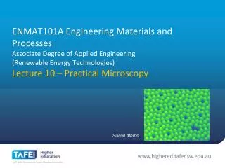
ENMAT101A Engineering Materials and Processes Associate Degree of Applied Engineering (Renewable Energy Technologies) Lecture 10 – Practical Microscopy. Silicon atoms. Metallographic Sample Preparation: (Higgins Ch 10). Following closely with Higgins Ch 10.

E N D
ENMAT101A Engineering Materials and ProcessesAssociate Degree of Applied Engineering (Renewable Energy Technologies)Lecture 10 – Practical Microscopy Silicon atoms
Metallographic Sample Preparation: • (Higgins Ch 10) Following closely with Higgins Ch 10 EMMAT101A Engineering Materials and Processes
Selecting and mounting a specimen: (Higgins Ch 10.2) Grain orientation is important. Take care not to heat while cutting. Higgins EMMAT101A Engineering Materials and Processes
Selecting and mounting a specimen: (Higgins Ch 10.2) Specimens cast into thermoset in order to hold them easily and in the right orientation. http://www.lambdaphoto.co.uk EMMAT101A Engineering Materials and Processes
Grinding and polishing the specimen: (Higgins Ch 10.3) Grinding and Polishing Machine for Metallographic Sample Preparation http://www.youtube.com/watch?v=yYiXfYwX1Ls Successively finer grades until specimen is finally polished with diamond paste. The most important points to be observed during the grinding and polishing processes are: • Absolute cleanliness is necessary at each stage. • Use very light pressure during both grinding and polishing. EMMAT101A Engineering Materials and Processes
Etching the specimen: (Higgins Ch 10.4) When the specimen is clean and free from grease, it is etched by plunging it into the etching solution (acid), and agitating it vigorously for a few seconds. The specimen is then very quickly transferred to running water. The highly polished surface will now appear dull. Grains may be visible if they are large (steel specimens need a microscope). Different etchants are used for different metals. EMMAT101A Engineering Materials and Processes
The metallurgical microscope: (Higgins Ch 10.5) Metallurgical microscope is lit on the front of the specimen, rather than through the back of a thin slice like a biological microscope. Optical microscope can only go so far – at x1000 magnification the resolution is down to the wavelength of light, which is the theoretical limit. Well before the x1000 limit, the definition depends on the objective lense (nearest the specimen). So several hundred magnification is more likely the maximum. Read Higgins: 10.5.1 Using the microscope 10.5.2 The care of the microscope EMMAT101A Engineering Materials and Processes
Photomicrographs: Images from a metallurgical microscope. (refer website) Photographs though a microscope are called Metallographics Metallurgical photos Micrographic images watlas.mt.umist.ac.uk/internetmicroscope/micrographs/microstructures.html EMMAT101A Engineering Materials and Processes
Revision From Lecture 1Nanometerscale FDA EMMAT101A Engineering Materials and Processes
Online Scale of the Universe http://scaleofuniverse.com/ Interactive flash animation from 10-35 m to 1027 m. (But more manageably; picameters to terameters) EMMAT101A Engineering Materials and Processes
50 nanometer diameter optical fibre transmits light while wrapped around a human hair. Optical microscope image: Limin Tong/Harvard University Optical microscope limited to a resolution of about 200nm. EMMAT101A Engineering Materials and Processes
The electron microscope: (Higgins Ch 10.6) The electron microscope can magnify x2000 and up to about x200 000. To see atoms, the magnification would need to be about twenty million times: x20 000 000 – a hundred times higher than the limit of the SEM. When did scientists first start to see atoms? "We are crossing that threshold where we can really see atoms clearly for the first time ever” This was in 2004. EMMAT101A Engineering Materials and Processes
Human hair is about 50mm or 0.05 mm. This nanowire (a fibre-optic glass wire) is about 50 nanometers, or 0.05 mm or 0.00005 mm. SEM image: Limin Tong/Harvard University EMMAT101A Engineering Materials and Processes
That last image was done on a Scanning Electron Microscope, which is more powerful than optical microscope. Wikipedia EMMAT101A Engineering Materials and Processes
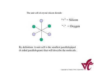
The electron microscope: (Higgins Ch 10.6) When did scientists first start to see atoms? "We are crossing that threshold where we can really see atoms clearly for the first time ever” This was in 2004. We can’t really “see” them, but we can visualize or “feel” them. But we are just starting to get pictures of molecules and atomic lattices. Here, an STM image of silicon atoms arranged on a face of a crystal. STM: http://www.sljus.lu.se/stm/NonTech.html EMMAT101A Engineering Materials and Processes
The STM microscope: The microscope is rather like an extremely accurate record player. It works by holding a very fine needle or tip approximately a billionth of a meter (1 nanometer) from the sample's surface. When the tip is this close, electrons can jump the gap between it and the sample. This 'tunnel current' can be amplified and used to measure the size of the gap with tremendous accuracy. Using electronic feedback system to keep the current (and hence the gap) constant as the tip moves sideways across the surface. Because the current detection is so sensitive the tip actually has to ride up over the atoms of the surface in exactly the same way that a record player's stylus tracks the groove of an LP. By recording the tip's vertical position at points on a grid we can make a 3D map of the surface. A computer then takes this map and turns it into a picture. Scanning Tunneling Microscope STM: http://www.sljus.lu.se/stm/NonTech.html EMMAT101A Engineering Materials and Processes
Opensource Handbook of Nanoscience and Nanotechnology (SEM) A: an ant 'looking' on a microchip (but it’s dead), B: cantilevers on a microchip touch a carbon nanotube substrate. C: closeup of carbon nanotubes electron beam deposition welded to the microscantilevers; (TEM) D: multiwalled carbon nanotube actually suspended between two microcantilevers. E: closeup of shell structure of the carbon nanotube. EMMAT101A Engineering Materials and Processes
Carbon Nanostructures. Nanotechnology is usually 10 to 100 nanometers. Polymorphism Allotropes of Carbon a) Diamond b) Graphite c) Lonsdaleite d) C60 (Buckminsterfullerene) e) C540 (see Fullerene) f) C70 (see Fullerene) g) Amorphous carbon h) single-walled nanotube Wikipedia EMMAT101A Engineering Materials and Processes
Online Properties Resources. Graphical comparison of materials properties. DoITPoMS: Dissemination of IT for the Promotion of Materials Science Wikipedia: Materials properties watlas.mt.umist.ac.uk/internetmicroscope/micrographs/microstructures.html Scales of material structure EMMAT101A Engineering Materials and Processes
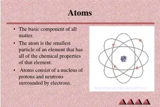
GLOSSARY Metallographic Metallurgical Micrographic Micrographic specimen Etching Optical Microscope Scanning Electron Microscope (SEM) Magnification Objective Lense Scanning Tunnelling Microscope (STM) Nanometer
QUESTIONS Define the glossary terms Explain how atoms can be “seen” using STM. What causes the theoretical limit of the magnification of an optical microscope? Describe some of the limitations when working with a SEM. Why is it important not to overheat a metallic specimen when cutting it in preparation for metallographic imaging? Why is cleanliness important in polishing metallurgical specimens for microscopy?