Download
1 / 3
0 likes | 18 Views
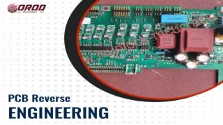
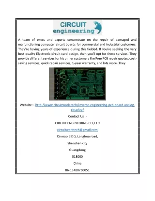
PCB Reverse Engineering" specializes in providing comprehensive reverse engineering services for printed circuit boards (PCBs). With expertise in deciphering intricate PCB designs, our team meticulously analyzes and reconstructs electronic schematics and layouts. Whether you need to replicate obsolete PCBs, troubleshoot issues, or enhance product performance, our reverse engineering solutions offer efficient and cost-effective alternatives. Trust us to unlock the secrets of your PCBs and deliver accurate, tailored solutions to meet your needs.

E N D
From Concept to Reality Leveraging PCB Reverse Engineering Services Introduction: In an era where innovation reigns supreme, the ability to understand, replicate, and improve upon existing technologies is paramount. PCB (Printed Circuit Board) Reverse Engineering stands at the forefront of this endeavor, offering a gateway to unraveling the complexities of electronic devices. As a pioneering provider of Reverse Engineering Services, we delve into the depths of technology to empower businesses with insights and solutions that drive progress. Understanding PCB Reverse Engineering: At its core, PCB Reverse Engineering is the process of dissecting and analyzing the architecture, functionality, and components of a printed circuit board to discern its design, functionality, and schematics. This intricate process requires a blend of technical expertise, advanced tools, and a meticulous approach to unravel the intricacies embedded within the circuitry. The Process Initial Assessment: We begin by conducting a thorough assessment of the client's requirements and the target device. This phase involves gathering relevant documentation, examining the physical characteristics of the PCB, and identifying key components. PCB Imaging: High-resolution imaging techniques such as X-ray imaging, scanning electron microscopy (SEM), or optical microscopy are employed to capture detailed images of the PCB's layers and components. These images serve as the foundation for subsequent analysis. Schematic Extraction: Through meticulous examination and analysis of the captured images, our experts reconstruct the schematic diagram of the PCB. This step involves identifying individual components, determining their interconnections, and documenting the circuitry. Component Identification: Utilizing advanced software tools and manual inspection, we identify each component on the PCB integrated circuits (ICs), resistors, capacitors, and connectors. Accurate component identification is
essential for understanding the functionality and behavior of the electronic system. Reverse Engineering Software: We leverage state-of-the-art software tools for PCB layout design and simulation to create virtual models of the reverse-engineered PCB. These digital representations enable us to validate the accuracy of the reconstructed schematic and layout, facilitating further analysis and modifications. Verification and Validation: The reconstructed schematic and layout undergo rigorous verification and validation processes to ensure alignment with the original design specifications. Any discrepancies or inconsistencies are meticulously addressed to achieve optimal accuracy. Documentation and Reporting: Upon completion of the reverse engineering process, comprehensive documentation and reports are generated, providing clients with detailed insights into the PCB's design, components, and functionality. These documents serve as invaluable resources for future reference and decision-making. The Importance of PCB Reverse Engineering: Innovation often hinges on the ability to understand existing technologies comprehensively. PCB Reverse Engineering serves as a catalyst for innovation by providing businesses with the opportunity to gain insights into competitor products, troubleshoot issues, and enhance product performance. Moreover, it enables legacy systems to be modernized, fostering sustainability and longevity in a rapidly evolving technological landscape. Our Approach to PCB Reverse Engineering: As a leading provider of Reverse Engineering Services, we employ a systematic approach that ensures accuracy, reliability, and efficiency throughout the process. Our team of seasoned engineers and technicians meticulously deconstruct PCBs, employing state-of-the-art tools and methodologies to extract vital information without compromising integrity. From schematic capture to component analysis, we leave no stone unturned in our quest to deliver actionable insights and solutions. Key Benefits of Partnering with Us:
Expertise: With years of experience and a proven track record, our team boasts unrivaled expertise in the field of PCB Reverse Engineering, ensuring superior results every time. Advanced Technology: Leveraging cutting-edge tools and techniques, we stay ahead of the curve, enabling us to tackle even the most complex reverse engineering challenges with precision and efficiency. Customized Solutions: We understand that every project is unique, which is why we tailor our solutions to meet the specific needs and objectives of our clients, ensuring maximum value and impact. Confidentiality and Security: We prioritize the confidentiality and security of our clients' proprietary information, implementing stringent measures to safeguard sensitive data throughout the reverse engineering process. Conclusion: In a world driven by innovation, PCB Reverse Engineering emerges as a powerful tool for unlocking new possibilities and driving progress. As a trusted partner in this journey, we are committed to empowering businesses with actionable insights and solutions that propel them towards success. Whether it's gaining a competitive edge, modernizing legacy systems, or enhancing product quality, our expertise and dedication make us the premier choice for all your PCB Reverse Engineering needs. Partner with us today and embark on a journey of innovation and excellence. For inquiries or to learn more about our services, please contact us E-mail: bevanpcb@outlook.com WhatsApp: +86-13378667812 Website: https://pcb-reverse-engineering.com/