Chapter 5-1. PN-junction electrostatics
Chapter 5-1. PN-junction electrostatics. In this chapter you will learn about pn junction electrostatics: Charge density, electric field and electrostatic potential existing inside the diode under equilibrium and steady state conditions. . You will also learn about: Poisson’s Equation

Chapter 5-1. PN-junction electrostatics
E N D
Presentation Transcript
Chapter 5-1. PN-junction electrostatics In this chapter you will learn about pn junction electrostatics: Charge density, electric field and electrostatic potential existing inside the diode under equilibrium and steady state conditions. • You will also learn about: • Poisson’s Equation • Built-In Potential • Depletion Approximation • Step-Junction Solution
PN-junction fabrication PN-junctions are created by several processes including: 1. Diffusion 2. Ion-implantation 3. Epitaxial deposition Each process results in different doping profiles
Equilibrium energy band diagram for the pn junction EF = same everywhere under equilibrium Join the two sides of the band by a smooth curve.
Electrostatic variables for the equilibrium pn junction Potential, V = (1/q) (EC–Eref). So, potential difference between the two sides (also called built-in voltage, Vbi) is equal to (1/q)(EC). = charge density = Ks o
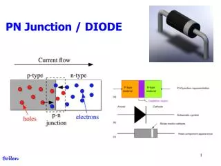
Conceptual pn-junction formation p and n type regions before junction formation Holes and electrons will diffuse towards opposite directions, uncoveringionized dopant atoms. This will build up an electric field which will prevent further movement of carriers.
The built-in potential, Vbi When the junction is formed, electrons from the n-side and holes from the p-side will diffuse leaving behind charged dopant atoms.Remember that the dopant atoms cannot move! Electrons will leave behind positively charged donor atoms and holes will leave behind negatively charged acceptor atoms. The net result is the build up of an electric field from the positively charged atoms to the negatively charged atoms, i.e., from the n-side to p-side. When steady state condition is reached after the formation of junction (how long this takes?) the net electric field (or the built in potential) will prevent further diffusion of electrons and holes. In other words, there will be drift and diffusion currents such that net electron and hole currents will be zero.
hole diffusion current net = 0 hole drift current Equilibrium conditions Under equilibrium conditions, the net electron current and hole current will be zero. E-field NA = 1017 cm3 ND = 1016 cm3 electron diffusion current opposite to electron flux net = 0 electron drift current opposite to electron flux
EC Ei EV EC Ei EV The built-in potential, Vbi p-side n-side q Vbi = (Ei EF)p-side + (EF Ei)n-side
The built-in potential, Vbi The built-in potential, Vbi, measured in Volts, is numerically equal to the “shift” in the bands expressed in eV. Vbi = (1/q) {(Ei EF)p-side + (EFEi)n-side } An interesting fact:
Majority and minority carrier concentrations p-side NAND n-side pp nn pn np x xp xn
Built-in potential as a function of doping concentration for an abrupt p+n or n+p junction
Depletion approximation Poisson equation We assume that the free carrier concentration inside the depletion region is zero.
Example 1 A p-n junction is formed in Si with the following parameters. Calculate the built-in voltage, Vbi. ND = 1016 cm–3 NA = 1017 cm–3 Calculate majority carrier concentration in n-side and p-side. Assume nn = ND = 1016 cm3 and pp=NA= 1017 cm3. Plug in the numerical values to calculate Vbi.
ND = 21016 cm-3 NA = 3 1017 cm-3 NA = 1016 cm-3 ND = 2 1017 cm-3 Example 2 A pn junction is formed in Si with the following parameters. Calculate the built-in voltage, Vbi. Calculate majority carrier concentration in n-side and p-side. nn=“effective ND” = 1016 cm-3. pp = “effective NA”=1017 cm–3. Here NA and ND are “effective” or net values. Plug in the numerical values to calculate Vbi.