Download
1 / 26
930 likes | 6.14k Views
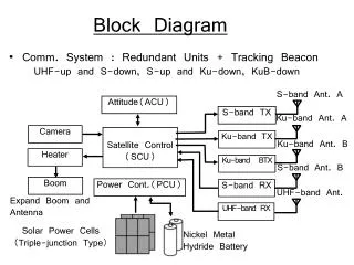
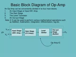
Basic Block Diagram of Op-Amp. V 1. Out put Stage (Buffer). Level Shifter. Gain Stage (C E Amp.). Input Stage (Diff. Amp.). I / P. V O. An Op-Amp can be conveniently divided in to four main blocks An Input Stage or Input Diff. Amp. The Gain Stage The Level Translator An Out put Stage

E N D
Basic Block Diagram of Op-Amp V1 Out put Stage (Buffer) Level Shifter Gain Stage (C E Amp.) Input Stage (Diff. Amp.) I/P VO An Op-Amp can be conveniently divided in to four main blocks An Input Stage or Input Diff. Amp. The Gain Stage The Level Translator An Out put Stage Note: It can be used to perform various mathematical operations such as Addition, Subtraction, Integration, Differentiation, log etc. V2 Op-Amp IC
An IDEAL OP AMP An ideal op amp has the following characteristics: • Infinite open-loop voltage gain, AV≈ ∞. • Infinite input resistance, Ri≈∞. • Zero output resistance, Ro≈ 0. • Infinite CMRR, ρ =∞ • The output voltage Vo=0; when Vd = V2-V1= 0 • Change of output with respect to input, slew rate = ∞ • Change in out put voltage with Temp., ∂Vo/∂Vi=0
The Operational Amplifier +VS _ i(-) Inverting RO A vid Output Ri vO = AdVid Noninverting i(+) + -VS • i(+), i(-) : Currents into the amplifier on the inverting and non-inverting lines respectively • vid : The input voltage from inverting to non-inverting inputs • +VS , -VS : DC source voltages, usually +15V and –15V • Ri : The input resistance, ideally infinity • A : The gain of the amplifier. Ideally very high, in the 1x10¹⁰ range. • RO: The output resistance, ideally zero • vO: The output voltage; vO = AOLvid where AOL is the open-loop voltage gain
+ - Operational Amplifier Model • An operational amplifier circuit is designed so that • Vout = Av(V1-V2) (Avis a very large gain) • Input resistance (Rin) is very large • Output resistance (Rout) is very low V1 Rout Vout Rin Av(V1- V2) V2
Practical Op-Amp Circuits These Op-amp circuits are commonly used: • Inverting Amplifier • Noninverting Amplifier • Unity Follower • Summing Amplifier • Integrator • Differentiator
Inverting Op-Amp Slide 7
Noninverting Amplifier Notice the output formula is similar to Inverting Amplifier, but they are not the same.
Summing Amplifier Because the op-amp has a high input impedance the multiple inputs are treated as separate inputs.
Inverting Amplifier: Input and Output Resistances Rout is found by applying a test current (or voltage) source to the amplifier output and determining the voltage (or current) after turning off all independent sources. Hence, vs= 0 But i1=i2 Since v- = 0, i1=0. Therefore vo= 0 irrespective of the value of io.
Differential Amplifier Using Op Amp I/P Current to op amp is zero
The Unity-Gain Amplifier or “Buffer” • This is a special case of the non-inverting amplifier, which is also called a voltage follower, with infinite R1 and zero R2. • Hence Av = 1. • It provides an excellent electrical isolation while maintaining the signal voltage level. • The “ideal” buffer requires no input current and can drive any desired load resistance without loss of signal voltage. • Such a buffer is used in many sensor and data acquisition system applications.
Unity-Gain Buffer Closed-loop voltage gain Used as a "line driver" that transforms a high input impedance (resistance) to a low output impedance. Can provide substantial current gain.
Op-Amp Integrator Cont… Since the inverting input is at virtual ground Applying KCL at the inverting input i1+i2 = 0
Op-Amp Differentiator Cont… Since the inverting input is at virtual ground Applying KCL at the inverting input i1+i2 = 0 Differentiators are avoided in practice as they amplify noise
Instrumentation Amplifier NOTE Combines 2 non-inverting amplifiers with the difference amplifier to provide higher gain and higher input resistance. Gain can be varied by varying single resistor R1 Ideal input resistance is infinite because input current to both op amps is zero. The CMRR is determined only by Op Amp 3.
Finite Open-loop Gain and Gain Error This is the “ideal” voltage gain of the amplifier. If Ab is not >>1, there will be “Gain Error”. is called the feedback factor.
Gain Error is given by GE = (ideal gain) - (actual gain) For the non-inverting amplifier, • Gain error is also expressed as a fractional or percentage error.
Output Voltage and Current Limits Practical op amps have limited output voltage and current ranges. Voltage: Usually limited to a few volts less than power supply span. Current: Limited by additional circuits (to limit power dissipation or protect against accidental short circuits). The current limit is frequently specified in terms of the minimum load resistance that the amplifier can drive with a given output voltage swing. Eg: For the inverting amplifier,