Metamaterials
Metamaterials. Prototype Showcase. What is a metamaterial? How our 2-D sample was created How our phase mask was created SEM images of 2-D sample and phase mask. Metamaterials. A periodic material that has photonic or phononic properties.


Metamaterials
E N D
Presentation Transcript
Prototype Showcase • What is a metamaterial? • How our 2-D sample was created • How our phase mask was created • SEM images of 2-D sample and phase mask
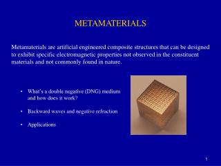
Metamaterials A periodic material that has photonic or phononic properties. *Taken From 3.042 handout & Physics Worlds 2005 “Sound Ideas”
Deliverables • 3-D periodic structure with micro-scale periodicity • Macro-scale representations of the structures
Prototype Design 2-D structure phase mask 3-D structure 3-D structure: Very thick (~50 microns) Variable spacing 2-D structure: 2 microns thick, 5 microns thick, 15 microns thick Variable spacing
Contact Lithography Coat soft bake @95° to evaporate solvent and cut into pieces coat with SU-8 2015 photoresist using spin coater coat with HMDS to make Si wafer hydrophobic plain Si wafer post bake at first 65° then 95° to promote crosslink formation Exposure UV exposure for either 15, 20, 25, or 30 seconds flip 90° and expose again submerge in isopropanol to wash away all remnants—final structure submerge in PM acetate to dissolve unexposed photoresist (20 min) Develop
Phase mask Vacuum sample with open bottle of fluorosilane so that it evaporates onto sample. Step 1 Step 2 Layer with PDMS and heat at 65°to 75°for at least three hours. Step 3 Gently peel off PDMSlayer as phase mask.
Fabrication and Processing Type of Photoresist SU-8 2015: 15 seconds, 20 seconds, 25 seconds, 30 seconds, 35 seconds, 40 seconds, 45 seconds SU-8 2005: 25 seconds, 30 seconds, 35 seconds, 40 seconds SU-8 2002: 15 seconds, 20 seconds, 25 seconds
Prototype Functionality Thick Film Photoresist Calculation: Sin (70) = 58 / t Thickness (t) ~ 61 microns Success!
Prototype Functionality 2-D Patterns Top-down view: Hole Spacing ~ 3.38 um Hole Length ~ 1.56 um Hole Height ~ 1.54 um Cross-section view: Width of top ~ 1.81 um Width of bottom ~ 1.00 um Height ~ 10.00 um
Prototype Functionality Problems in 2-D patterns Over exposure Un-washed monomer Non-uniform columns Width of top ~ 1.81 um Width of bottom ~ 1.00 um
Prototype Functionality Phase mask
2-D Pattern Phase Mask 3-D Pattern CAD Model 3-D Printing Model ? Actual Sample