Download
1 / 14
140 likes | 270 Views
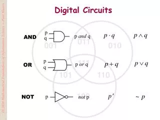
Digital Circuits to Compensate for Energy Harvester Supply Variation. Hao-Yen Tang. David Burnett. Energy-harvesting system. Battery Solar cell TEG(Thermoelectric) RF coupling Problem: voltage ripple. Voltage ripple. precharged. Energy Harvester. ~1nF. On-chip Storage cap.

E N D
Digital Circuits to Compensate forEnergy Harvester Supply Variation Hao-Yen Tang David Burnett
Energy-harvesting system • Battery • Solar cell • TEG(Thermoelectric) • RF coupling • Problem: voltage ripple
Voltage ripple precharged Energy Harvester ~1nF On-chip Storage cap VLSI block • Y. Ramadass and A. Chandrakasan, “A battery-less thermoelectric energy harvesting interface circuit with 35 mv startup voltage,” Solid-State Circuits, IEEE Journal of, vol. 46, no. 1, pp. 333–341, Jan. Energy harvester-powered integrated system
Possible solution • Work with minimum voltage • Supply regulation (with LDO) • Modified basic cells (Razor) • Dynamic clock period adjusting
Proposed solution HW2 decoder circuit (4x cascaded) Using a Delay-Lock Loop(DLL) to lock the clock period to critical path delay
Clock Generator (Voltage-Control Oscillator) • No crystal • Ring oscillator • Supply Sensitivity
Critical Path duplica • Extra delay result from simultaneous incoming signal • Need to be reset every cycle • 1 clock cycle measure1 clock cycle reset
PFD and loop filter • Traditional PFD • Charge pump with constant gm bias • Second order loop filter for stability
Simulation result Supply Voltage VCO control signal Extra power overhead: 40.2uW (12.7% of the reference VLSI block)
Acknowledgement • Prof. Bora <3 • EE241 classmates • Dear teammate